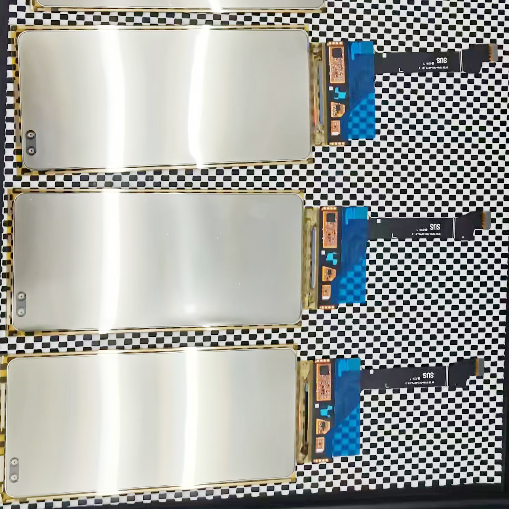
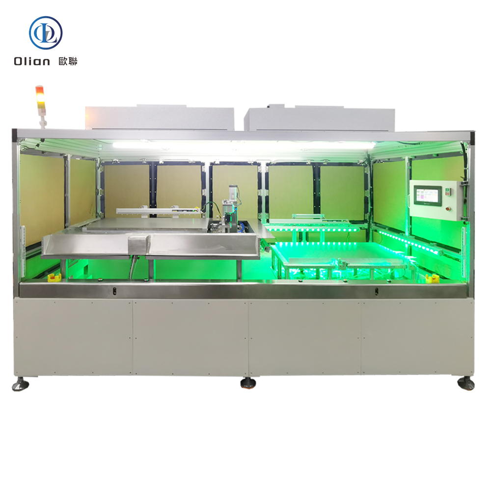
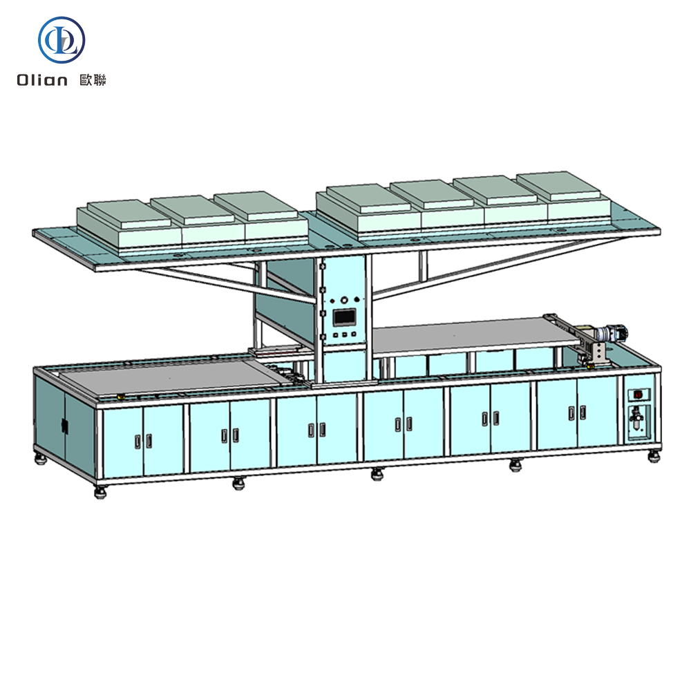
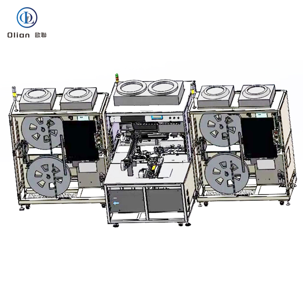
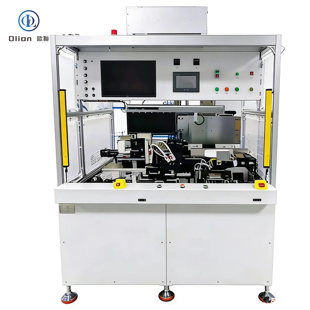
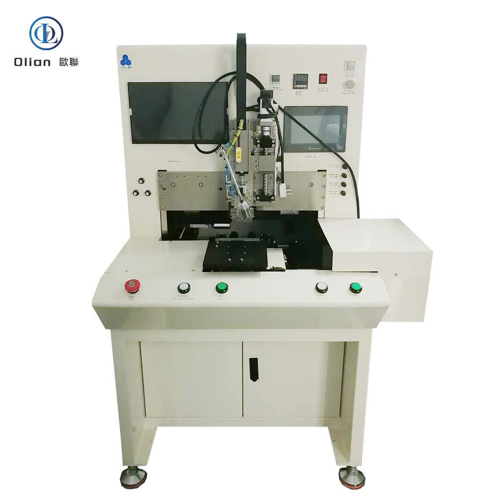
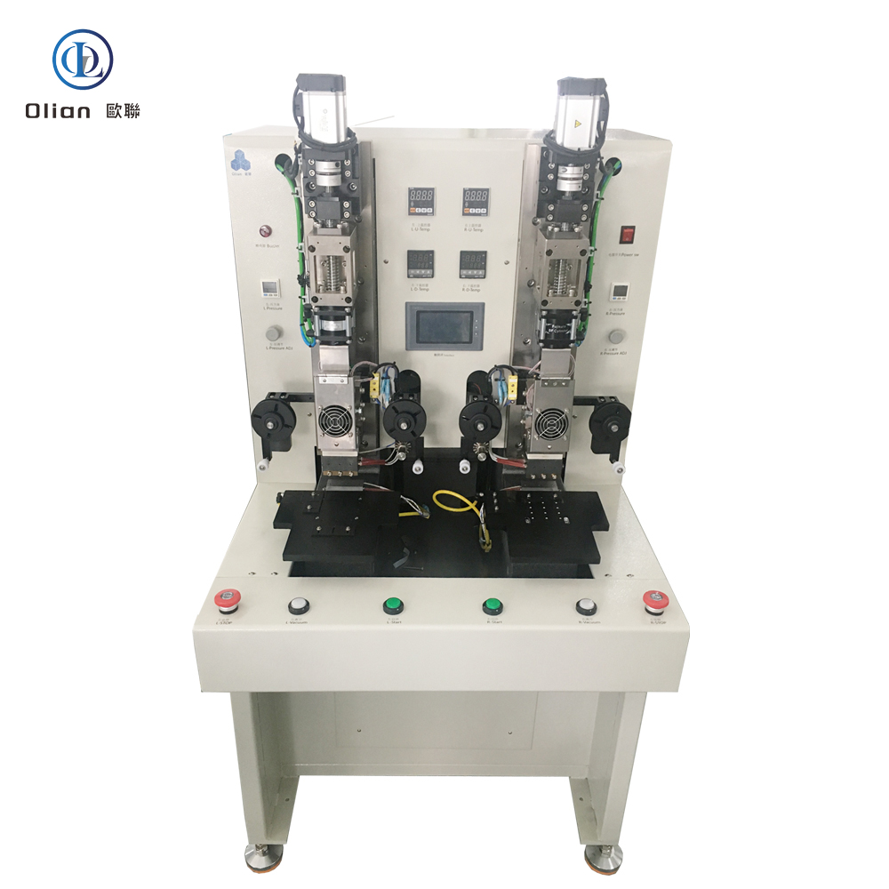
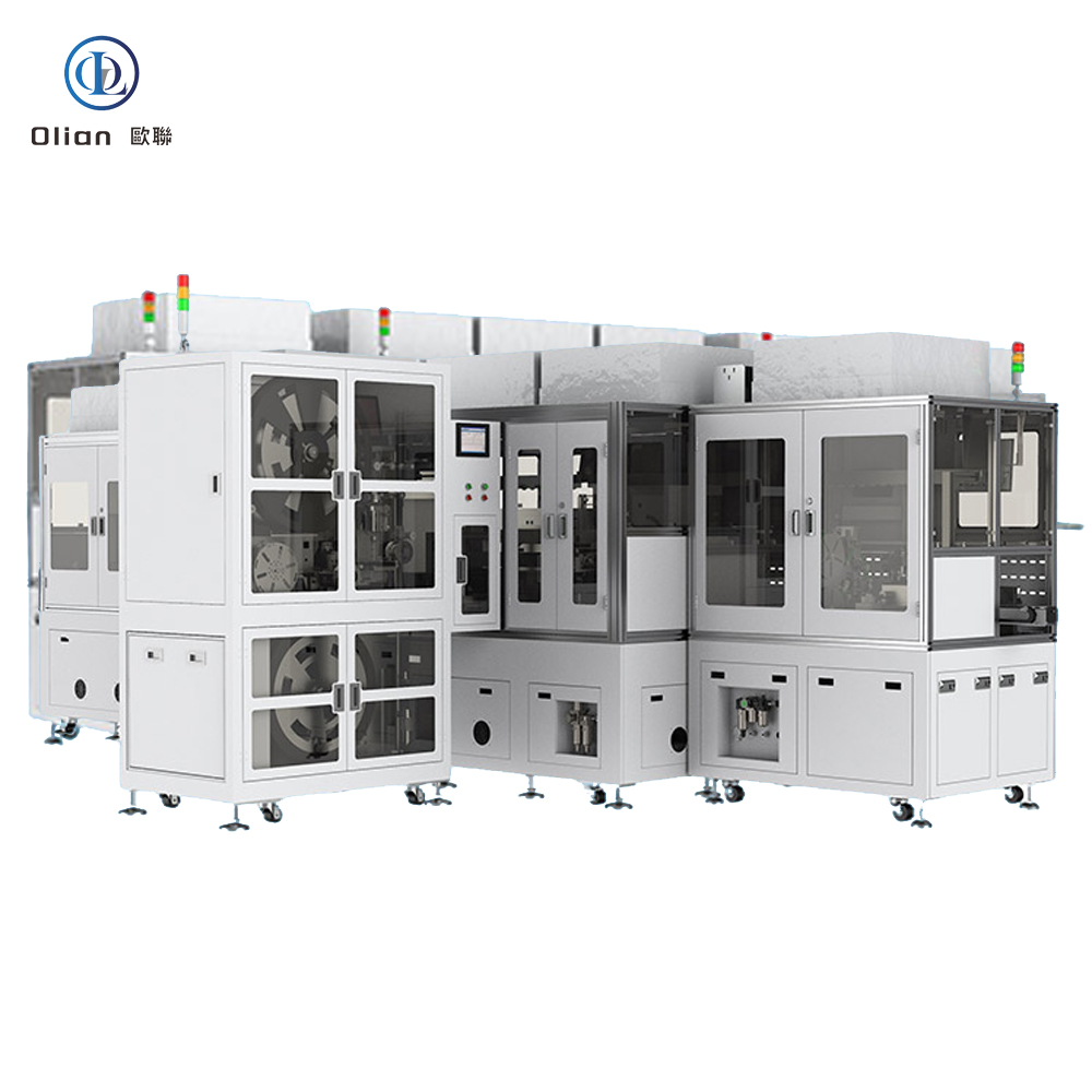
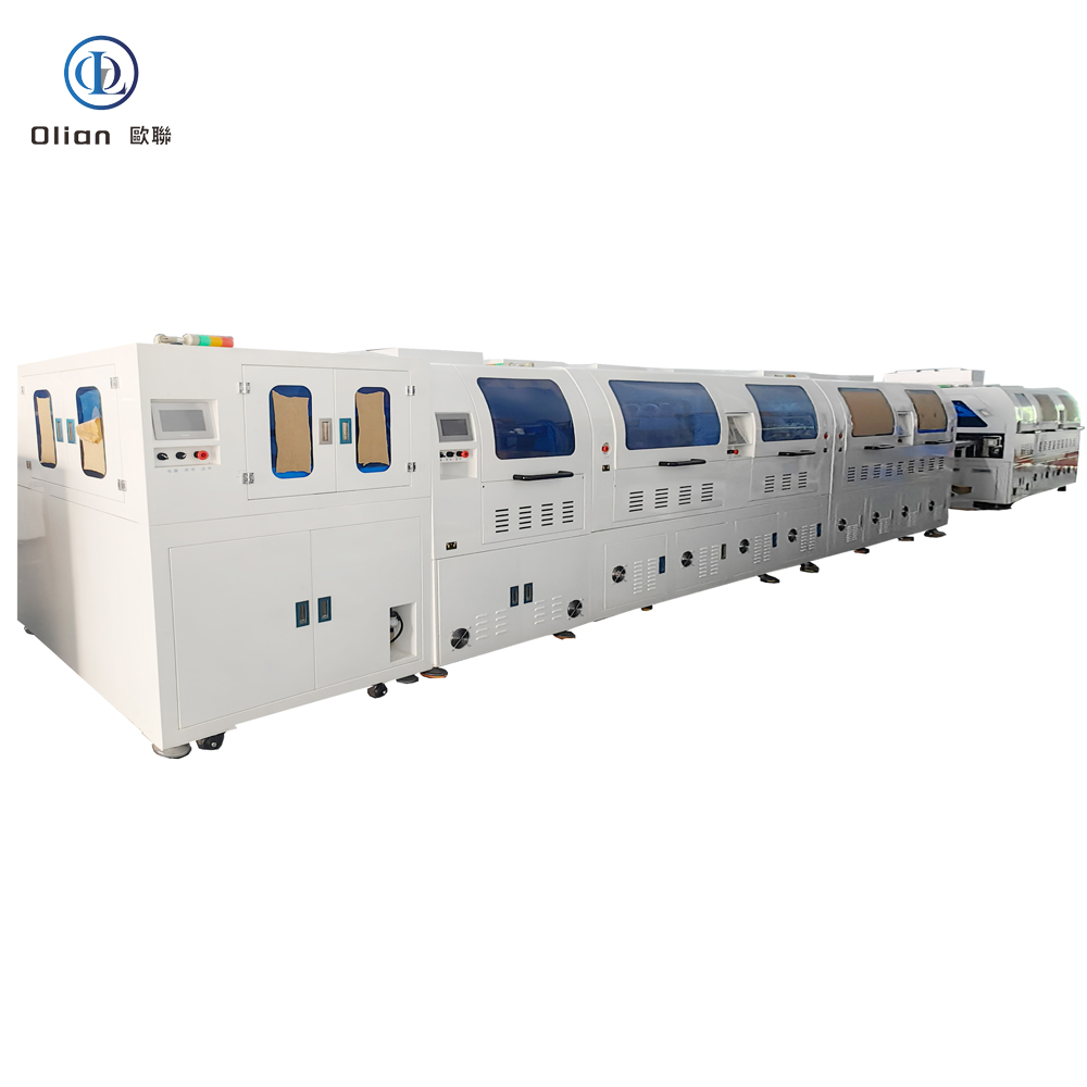
Flexible AMOLED Manufacturing: Full Process & Detailed Module Assembly
Clarification on AMOLED Technology
Before detailing the manufacturing workflow, it is crucial to clarify a fundamental technical distinction: AMOLED (Active-Matrix Organic Light-Emitting Diode) is a self-emissive display technology. Unlike LCDs, AMOLED screens do not require a backlight unit (BLU). Therefore, there is no “backlight assembly” step in this process. The complete production workflow is divided into four primary stages: Array, OLED Evaporation, Encapsulation, and Module Assembly.
1. Array Stage (TFT Backplane Fabrication)
This stage focuses on fabricating the driving circuits on a flexible substrate to provide precise electrical signals to each pixel.
Substrate Preparation: A Polyimide (PI) slurry is coated onto a temporary carrier glass and cured at high temperatures to form the flexible base.
Thin Film Deposition & Photolithography: Through 7 to 10 repetitive cycles of PECVD/PVD deposition, photolithography, and etching, the Low-Temperature Polysilicon (LTPS) TFT array circuits are constructed.
Pixel Definition Layer (PDL): Photosensitive PI is coated and patterned to precisely separate RGB sub-pixels and prevent color crosstalk.
Automated Optical Inspection (AOI): Advanced CDC equipment screens for circuit shorts, opens, and film defects.
2. OLED Stage (Vacuum Evaporation)
This is the core stage where organic light-emitting materials are precisely deposited into pixels under high vacuum.
Substrate Cleaning: Ultrasonic, chemical, and plasma treatments remove microscopic contaminants.
Vacuum Evaporation: At an ultra-high vacuum (10⁻⁶ to 10⁻⁷ Pa), a Fine Metal Mask (FMM) is used to sequentially evaporate the Hole Injection Layer (HIL), Hole Transport Layer (HTL), RGB Emitting Layers, Electron Transport Layer (ETL), and a semi-transparent cathode.
Light-Off Test (LOT): An initial power-on test is conducted immediately after evaporation to rapidly detect bright spots, dark spots, or bright lines.
3. Encapsulation Stage
Since organic materials are highly sensitive to moisture and oxygen, this stage provides a protective shield.
Thin Film Encapsulation (TFE): Alternating layers of inorganic materials (e.g., SiNx/Al₂O₃) and organic planarization layers (typically 3-6 layers) are deposited to achieve superior barrier properties.
Laser Lift-Off (LLO): An exclusive step for flexible screens. An excimer laser irradiates the back of the carrier glass, seamlessly separating the PI flexible substrate from the glass without damage.
Laser Cutting: The large panel is cut into individual cells using precision lasers, followed by edge grinding to prevent chipping.
4. Module Assembly Stage (In-Depth Breakdown)
This stage integrates the bare panel into a fully functional display module. It is the most complex phase involving precision mechanical and chemical processes.
A. Polarizer Attachment A Circular Polarizer (CPL) is laminated onto the panel to absorb ambient light reflections, significantly enhancing contrast and outdoor visibility.
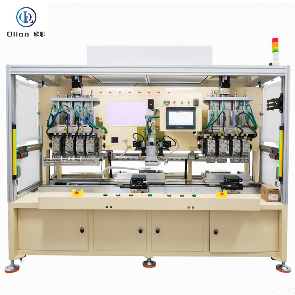
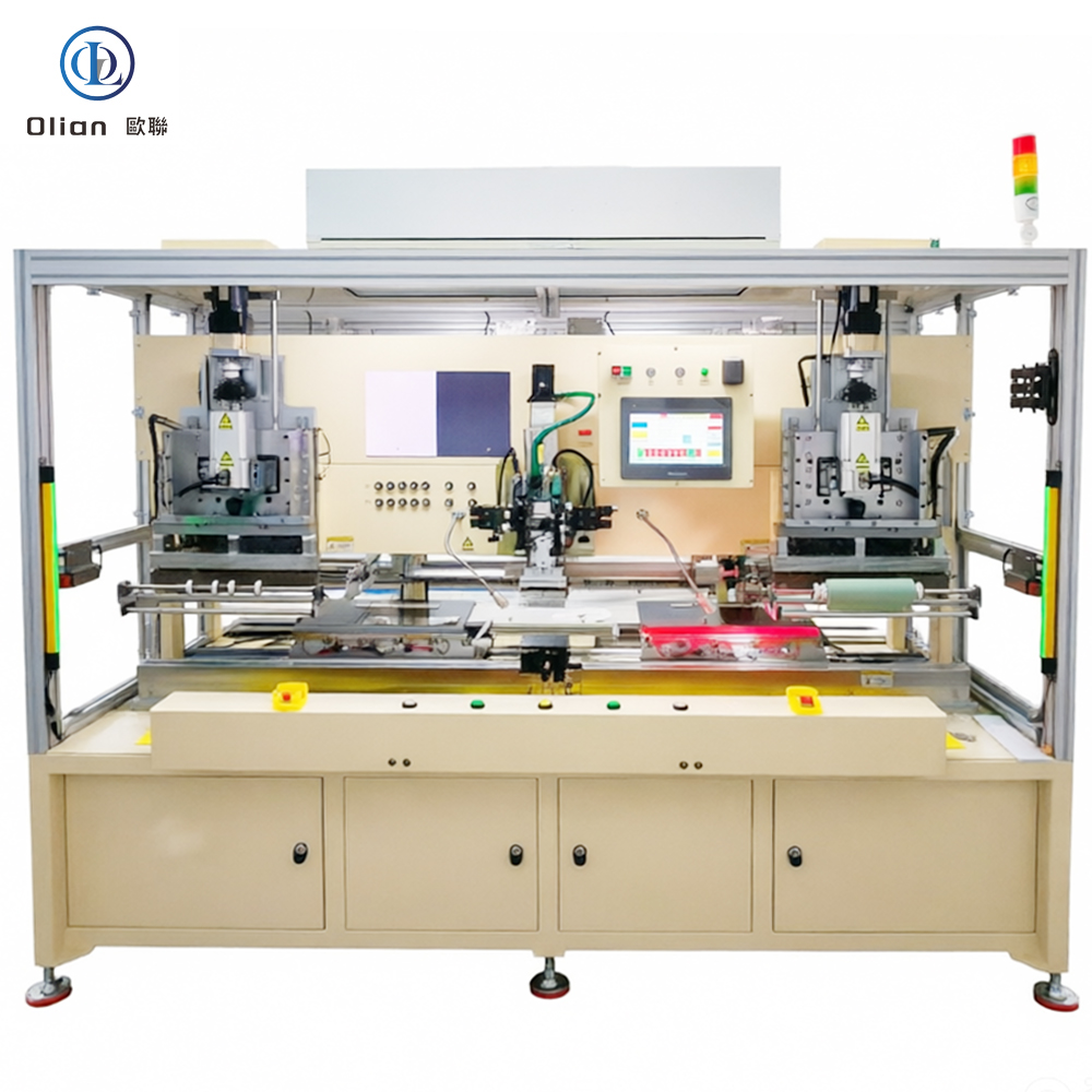
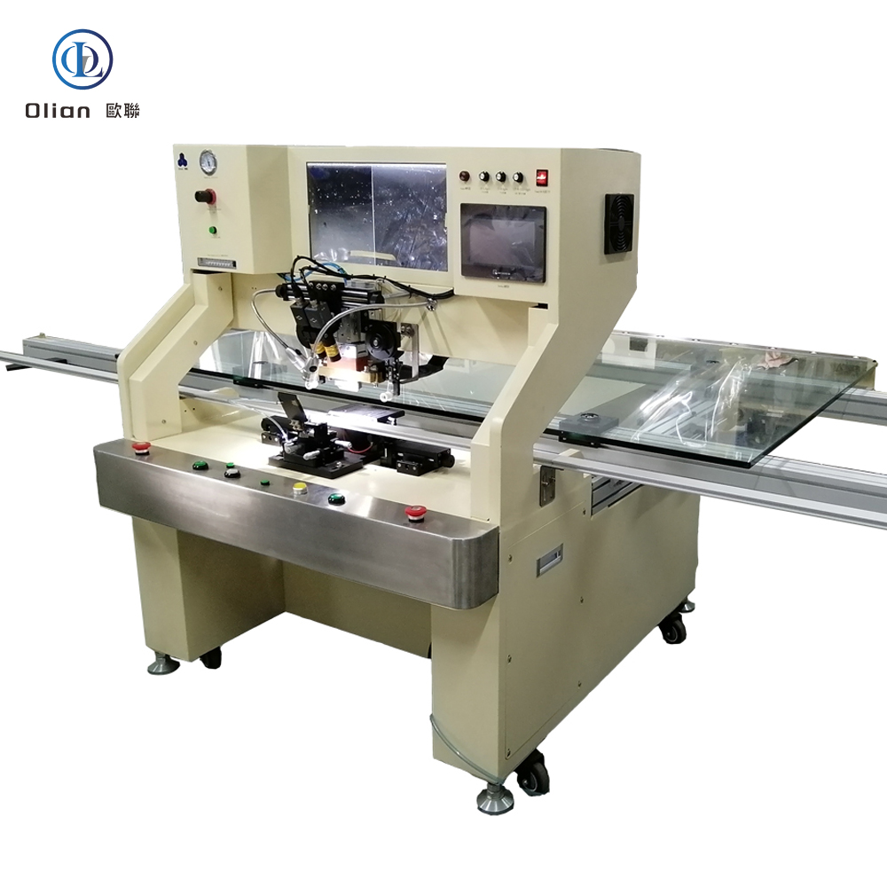
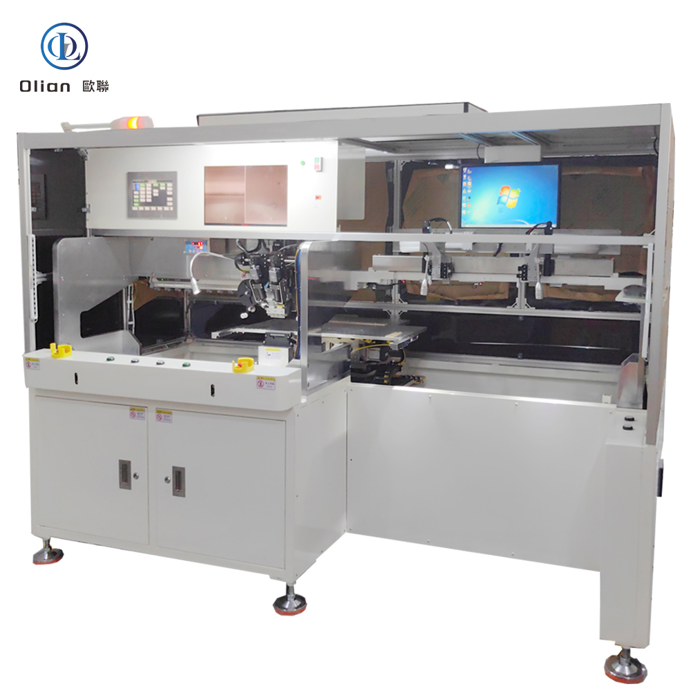
This step establishes the electrical connection between the display panel and external control systems.
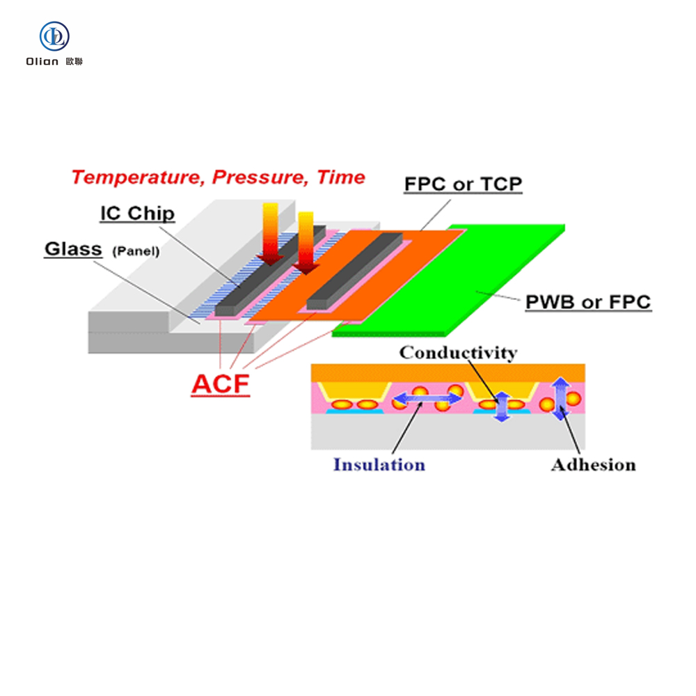
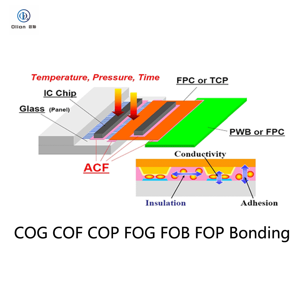
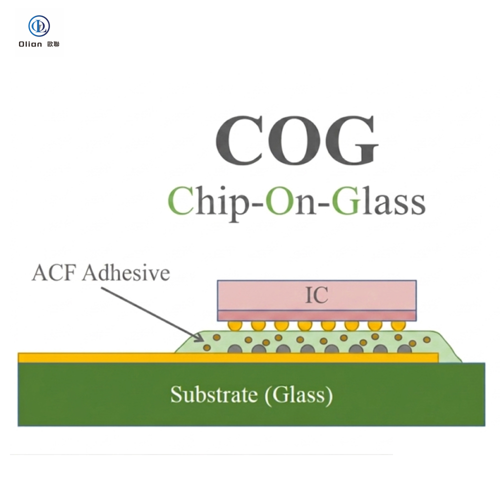
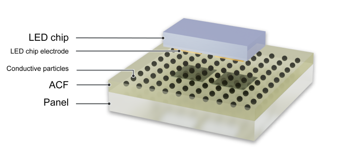
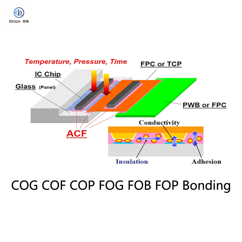
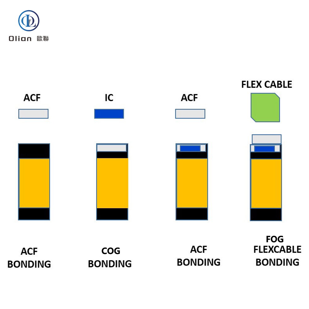
ACF Attachment: Anisotropic Conductive Film (ACF) is pre-bonded to the panel’s bonding pads. ACF contains conductive particles that ensure vertical electrical conductivity while providing horizontal insulation.
COF/COP Binding: The driver IC is aligned and thermally compressed onto the flexible film (or directly onto the panel). Critical parameters include temperature (typically 180°C-220°C), pressure, and dwell time to ensure optimal particle deformation and bonding strength.
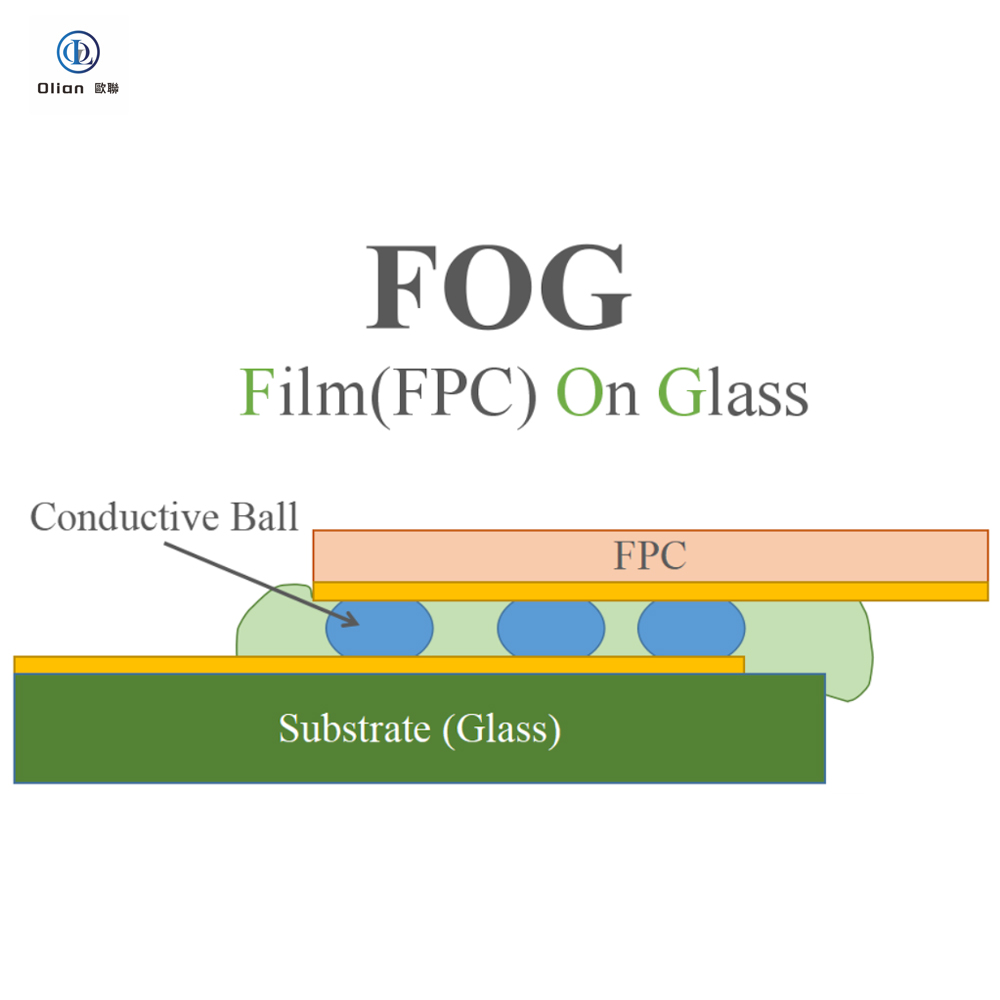
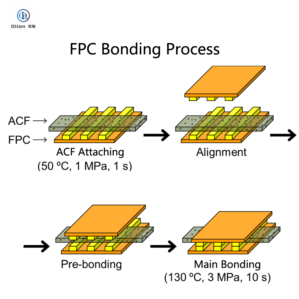
FPC Bonding: The Flexible Printed Circuit (FPC) is similarly aligned and hot-pressed to transmit signals.
AOI & Electrical Testing: Automated equipment checks for alignment shifts, ACF overflow, and conducts continuity/resistance tests to verify electrical pathways.
C. Dispensing & Sealing Process To protect vulnerable bonding areas and enhance structural integrity:
Edge Dispensing: UV-curable adhesives or epoxy resins are precisely dispensed along the edges of the cover glass or bonding regions using high-precision dispensing valves.
Curing: The adhesive is cured via UV light or thermal heating to form a hermetic seal, preventing moisture ingress and reinforcing the mechanical bond between layers.
D. Touch Integration & Optical Lamination Modern flexible AMOLEDs utilize On-Cell or In-Cell technology, integrating touch sensors directly into the panel or encapsulation layer.
Optical Bonding: The cover glass (such as Ultra-Thin Glass – UTG, or Colorless Polyimide – CPI) is seamlessly laminated to the AMOLED panel using OCA (Optically Clear Adhesive) or LOCA (Liquid Optically Clear Adhesive).
Deaeration & Curing: The assembly undergoes vacuum deaeration to eliminate air bubbles, followed by UV or autoclave curing. This step eliminates air gaps, improves light transmittance, reduces internal reflections, and significantly enhances drop-shock resistance.
E. Structural Assembly Double-sided tapes, foam pads, or metal brackets are applied to secure the module within the device’s frame, providing necessary cushioning for flexible bending zones.
5. Final Testing & Packaging
Module Functional Test (MFT): Comprehensive validation of display output, touch response, and signal transmission.
Optical & Color Calibration: Spectrometers measure brightness, color gamut, and uniformity. Demura compensation algorithms are applied to correct pixel-level brightness and color deviations.
Reliability Testing: Modules undergo rigorous stress tests, including high/low-temperature cycling, ESD testing, and flexible-specific folding tests (exceeding 200,000 cycles).
Final AOI & Packaging: A final visual and automated inspection ensures zero scratches or foreign particles before secure packaging for shipment.
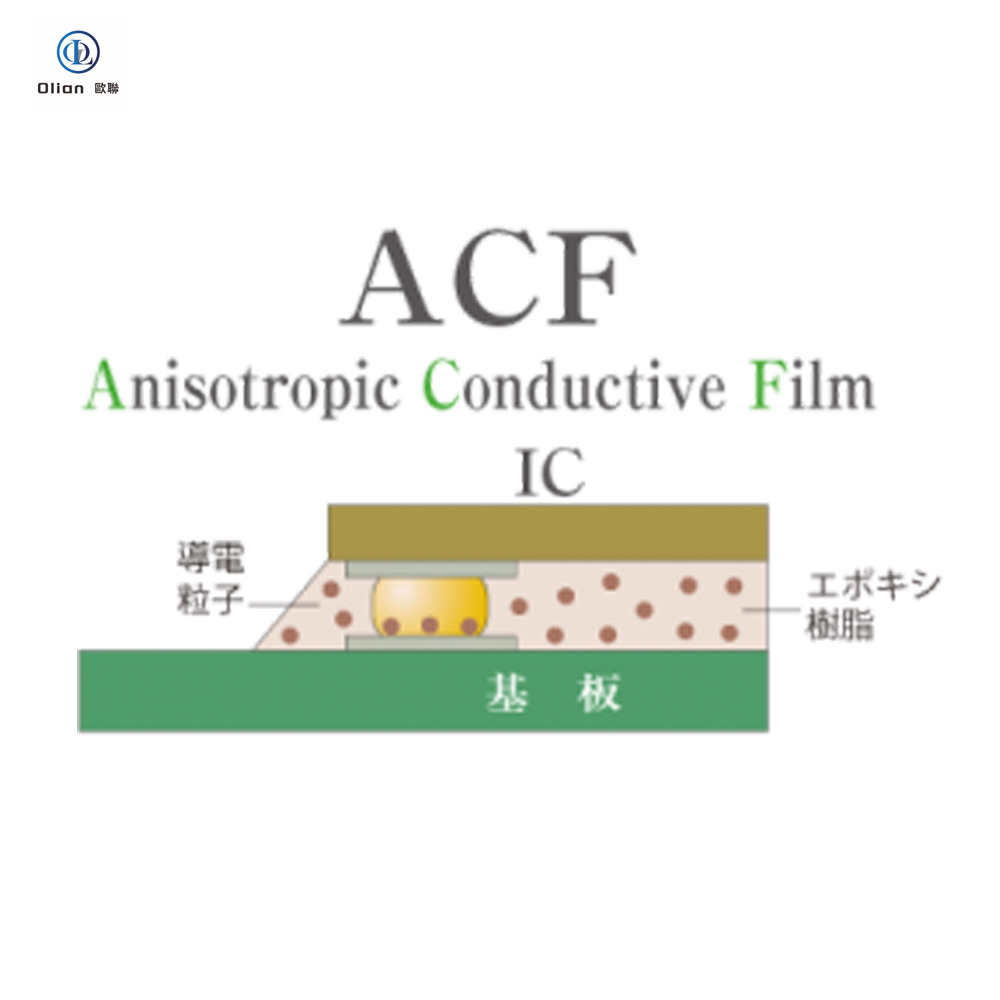
Anisotropic Conductive Film (ACF) is a specialized adhesive material. It contains conductive particles within an insulating resin. This unique structure allows vertical electrical conductivity. Simultaneously, it maintains horizontal insulation between circuits. ACF is essential for modern flat panel displays. It connects delicate components without short circuits. The film provides both adhesion and conduction. This dual function is critical for reliability. Olian Automatic utilizes this advanced material effectively. Our processes optimize the ACF performance. This ensures long-lasting display connections.
Core Bonding Processes Explained
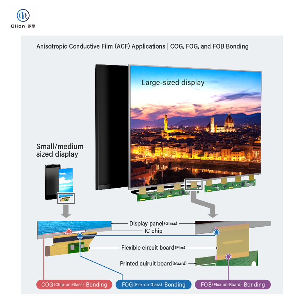
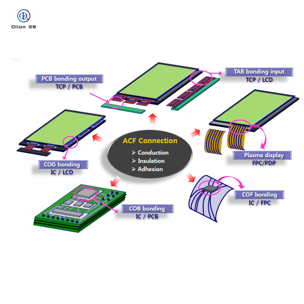
Several key bonding methods use ACF technology. Chip-on-Glass (COG) bonds IC chips directly to glass panels. This is common in LCD manufacturing. Chip-on-Film (COF) connects ICs to flexible circuits. This allows for thinner display bezels. Flex-on-Glass (FOG) attaches flexible boards to glass substrates. Flex-on-Board (FOB) connects flex circuits to rigid PCBs. Tape Automated Bonding (TAB) links TCP tapes to displays. Each process requires specific parameters. Olian Automatic masters all these techniques. We provide versatile solutions for various needs.
Glossary of ACF Bonding Terms
ACF (Anisotropic Conductive Film)
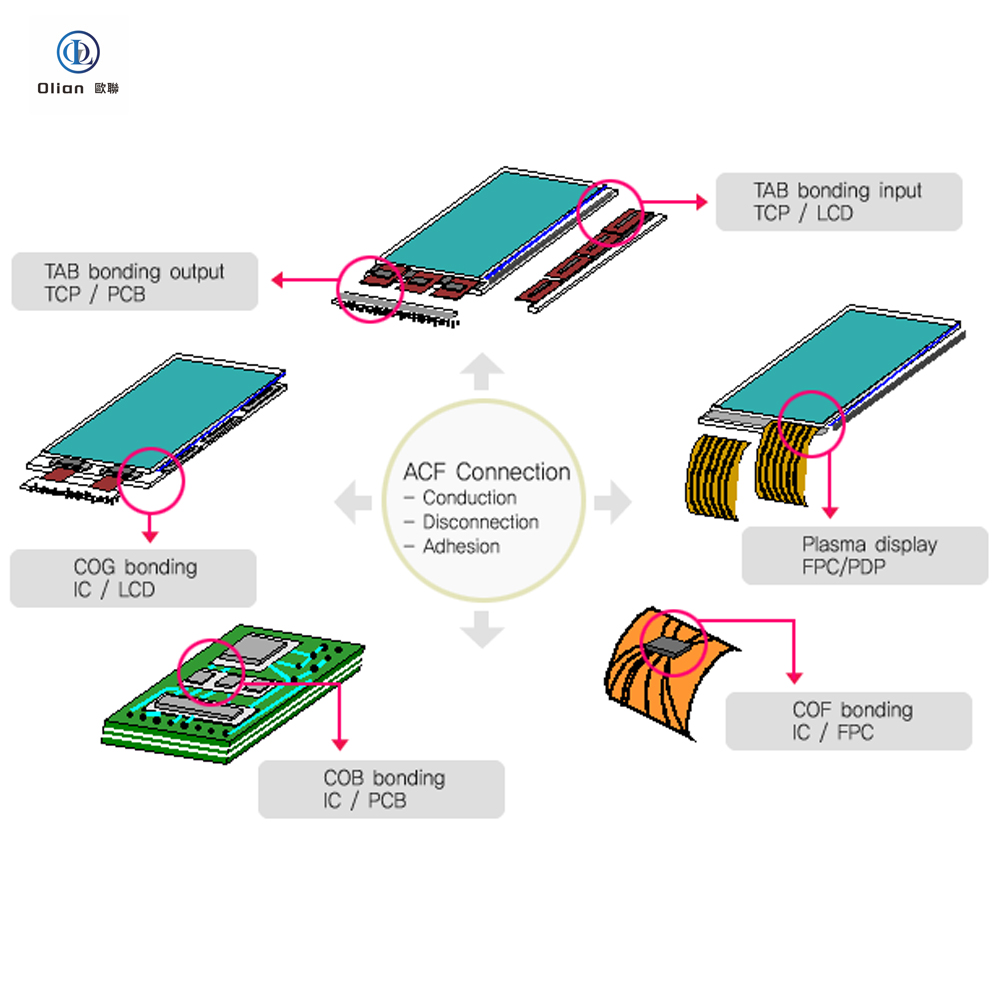
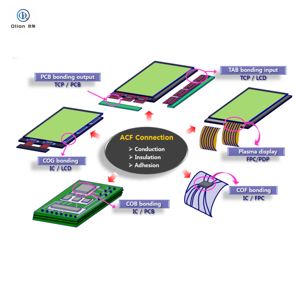
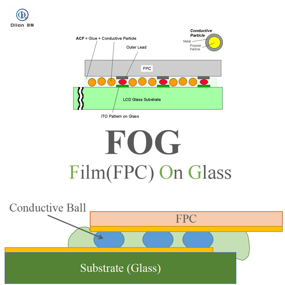
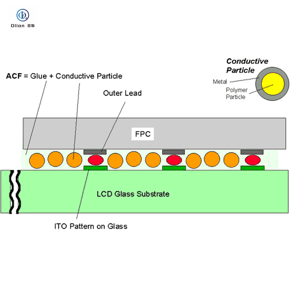
ACF stands for Anisotropic Conductive Film. It is a specialized adhesive material used in display assembly. The film contains conductive particles trapped in an insulating resin. It provides electrical conductivity in the vertical direction only. Simultaneously, it ensures electrical insulation in the horizontal direction. This unique property prevents short circuits between fine pitches. ACF also offers strong adhesion between components. It is the core material for COG, COF, and FOG bonding.
COG (Chip-on-Glass) Bonding
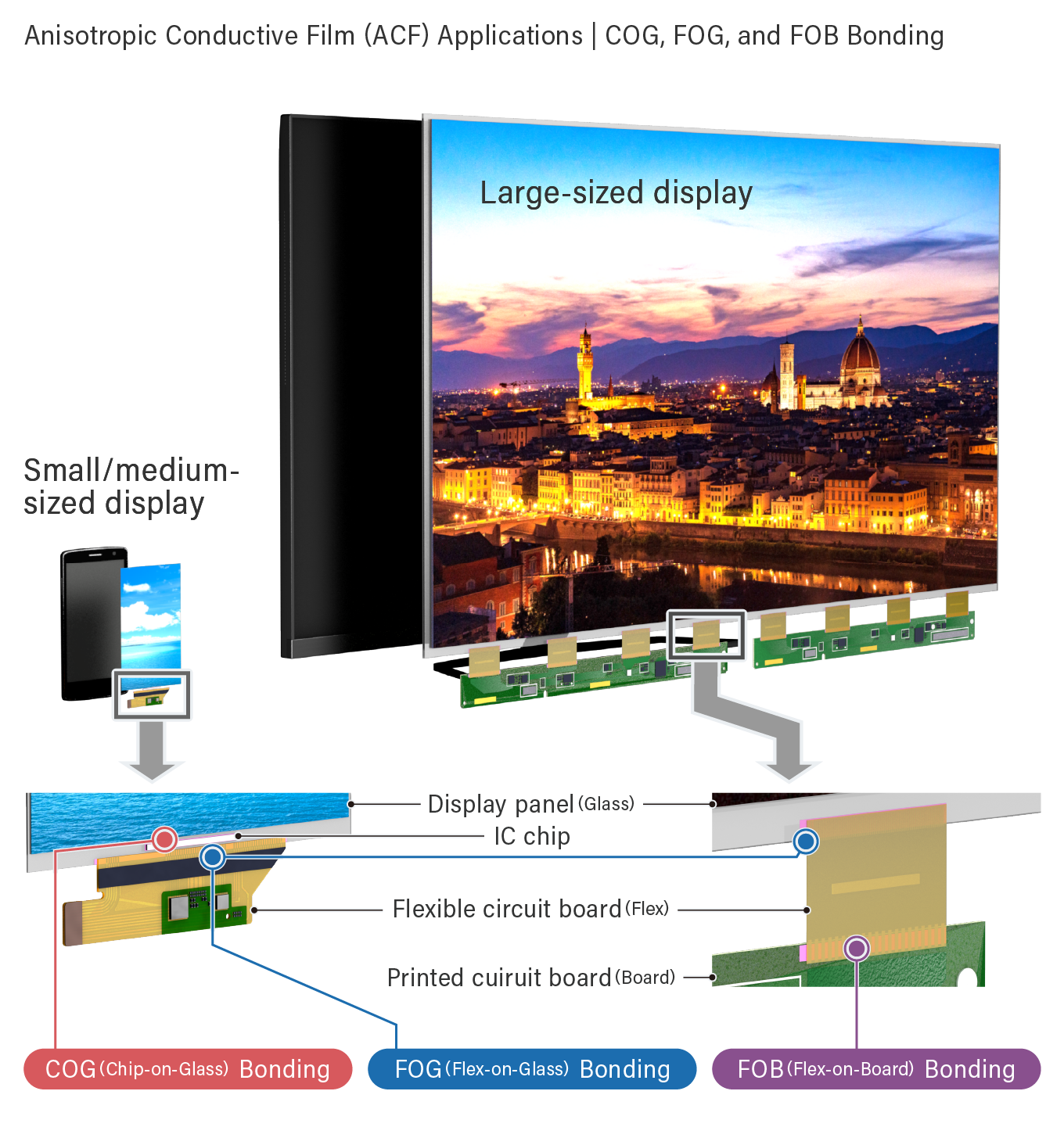
COG stands for Chip-on-Glass bonding. This process connects an IC chip directly onto a glass substrate. It is widely used in LCD and OLED panel manufacturing. The method eliminates the need for intermediate flexible tapes. COG bonding saves space and reduces module thickness. It requires precise alignment and controlled heat pressure. ACF is typically used as the interconnect material. This technique is common for source and gate driver ICs.
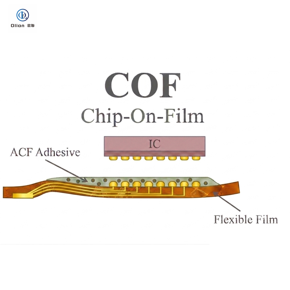
COF (Chip-on-Film) Bonding
COF stands for Chip-on-Film bonding. This technique mounts IC chips directly onto a flexible film. The film is usually a Tape Carrier Package (TCP). COF allows for very narrow display bezels. It enables the bending of the film under the panel. This creates a “bottom bezel” free design. The flexible circuit connects the glass to the main PCB. It supports high-resolution displays with many signal lines.
FOG (Flex-on-Glass) Bonding
FOG stands for Flex-on-Glass bonding. This process attaches a Flexible Printed Circuit (FPC) to a glass panel. It serves as the interface between the rigid glass and external electronics. FOG bonding is essential for transmitting signals to the display. It uses ACF to ensure reliable electrical connection. The process requires high precision to align fine circuit traces. It is a standard step in LCD module assembly.
FOB (Flex-on-Board) Bonding
FOB stands for Flex-on-Board bonding. This method connects a flexible circuit (FPC) to a rigid Printed Wiring Board (PWB). It bridges the gap between flexible and rigid electronics. FOB is often used in the final assembly stage. It links the display module to the main system board. The connection must withstand mechanical stress and bending. ACF provides both electrical continuity and mechanical strength.
COP (Chip-on-Plastic) Bonding
COP stands for Chip-on-Plastic bonding. Although less prominent in the diagrams, it is listed in the text. This technology bonds IC chips directly onto plastic substrates. It is increasingly used in flexible OLED displays. COP allows the entire display to be bendable or foldable. It replaces glass with polyimide or similar plastics. The bonding process requires lower temperatures to protect the plastic.
TCP (Tape Carrier Package)
TCP refers to Tape Carrier Package. It is a type of flexible interconnect technology. TCP carries IC chips on a thin polymer tape. It is the primary component used in COF bonding. The tape has fine metal leads for electrical connections. TCP allows for high-density packaging of driver chips. It acts as the bridge between the glass and the PCB.
FPC (Flexible Printed Circuit)
FPC stands for Flexible Printed Circuit. It is a lightweight, bendable electronic circuit board. FPCs are used in FOG and FOB bonding processes. They replace rigid cables to save space and weight. The circuit pattern is etched onto a flexible substrate. FPCs can route signals through tight spaces in devices. They are crucial for connecting moving or folded parts.
PWB (Printed Wiring Board)
PWB stands for Printed Wiring Board. It is commonly known as a rigid PCB. PWBs serve as the main backbone for electronic components. In display modules, PWBs receive signals from the FPC. FOB bonding connects the flexible display output to this board. PWBs provide mechanical support and complex circuit routing. They are essential for the final electronic assembly.
IC Chip (Integrated Circuit Chip)
IC Chip stands for Integrated Circuit Chip. In display bonding, these are typically driver ICs. They control the pixels on the screen to create images. The chip contains thousands of microscopic connection points. These points must align perfectly with the substrate pads. The IC is the “brain” of the display panel. Proper bonding is critical for its functionality.
Glass (Panel/Substrate)
Glass refers to the display panel substrate. It is the base material for LCD and OLED screens. The glass surface holds the pixel matrix and electrodes. COG and FOG bonding happen directly on this surface. The glass is fragile and requires careful handling. Cleanliness is vital before applying ACF. It provides a flat, stable platform for components.
Conductivity
Conductivity refers to the flow of electrical current. In ACF bonding, this happens vertically through the film. Conductive particles create the path between the chip and substrate. This ensures the signal reaches the display pixels. High conductivity is necessary for clear image quality. The resistance must be low and stable.
Insulation
Insulation prevents unwanted electrical flow. In ACF, the resin insulates adjacent signal lines horizontally. This prevents short circuits between neighboring traces. High insulation resistance is critical for fine-pitch connections. It ensures that signals do not cross paths. Reliable insulation guarantees the display functions correctly.
Adhesion
Adhesion is the mechanical sticking force of the bond. The ACF resin cures to hold components together firmly. Strong adhesion protects against moisture and dust ingress. It withstands thermal expansion and mechanical shock. Good adhesion ensures the long-term reliability of the device. It prevents the chip or film from peeling off.
Temperature, Pressure, Time
These are the three critical process parameters. Temperature activates the chemical curing of the ACF. Pressure forces the conductive particles into contact. Time determines the duration of the heat application. All three must be precisely controlled for a good bond. Incorrect settings lead to open circuits or weak joints. Olian Automatic systems optimize these variables perfectly.
TAB (Tape Automated Bonding)
TAB stands for Tape Automated Bonding. It is an older term often associated with TCP input. It refers to bonding the tape carrier to the LCD glass. The process uses heat and pressure to connect leads. TAB enables high-speed automated manufacturing. It is the precursor to modern COF technology.
Plasma Display
Plasma Display refers to PDP (Plasma Display Panel) technology. The images show FPC bonding for plasma displays. This indicates ACF’s versatility across different display types. Plasma panels also require reliable flex-to-glass connections. The bonding principles remain similar to LCDs. It demonstrates the broad application of Olian’s technology.
The Precision Bonding Workflow
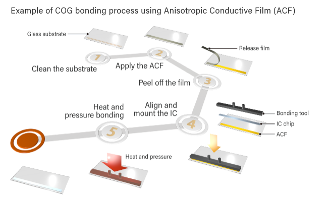
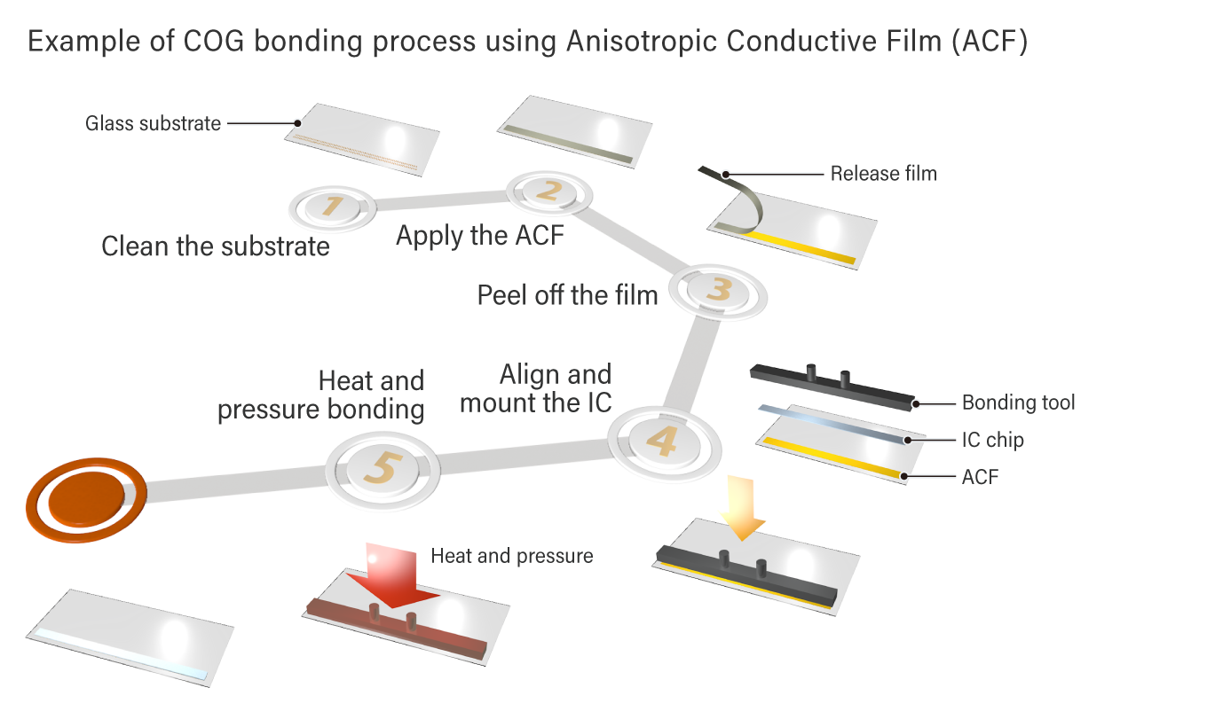
The ACF bonding process follows strict steps. First, technicians clean the glass substrate thoroughly. Next, they apply the ACF material carefully. Then, they peel off the protective release film. Precise alignment of the IC chip follows. Finally, heat and pressure are applied simultaneously. This activates the adhesive and conductive particles. The bonding tool ensures uniform pressure distribution. Temperature and time are strictly controlled. This five-step process guarantees perfect connections. Olian Automatic automates this workflow for consistency.
Applications Across Display Sizes
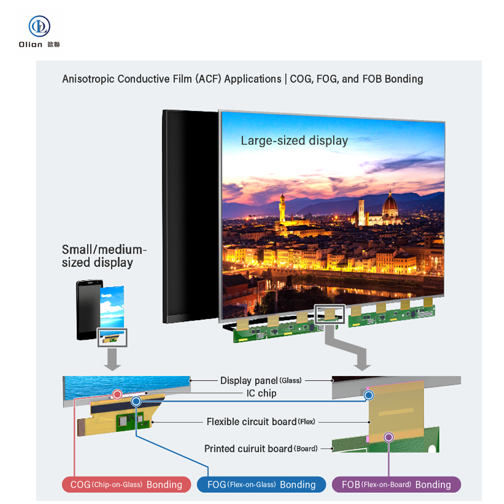
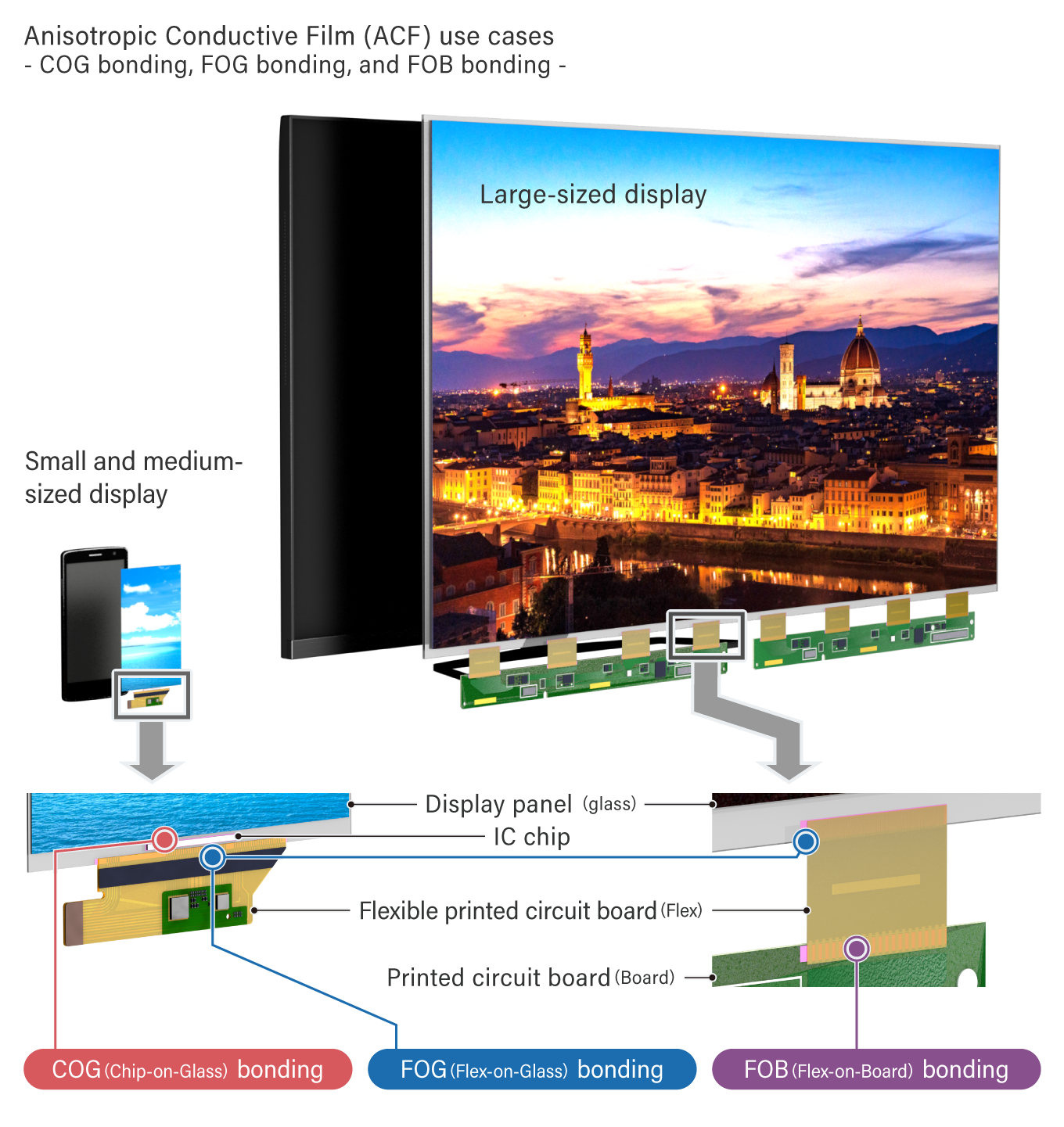
Our ACF bonding solutions serve diverse markets. Small and medium-sized displays utilize COG technology. Smartphones and tablets benefit from this method. Large-sized displays often require FOG and FOB bonding. Television screens use these robust connections. Plasma displays also rely on ACF technology. The flexibility of ACF supports curved screens. Olian Automatic adapts to all form factors. We support the entire display industry spectrum. Our equipment handles various panel sizes efficiently.
Why Choose Olian Automatic Solutions
Olian Automatic delivers superior bonding performance. Our systems ensure precise parameter control. Temperature, pressure, and time are optimized. This minimizes defects and maximizes yield. We understand the complexities of ACF materials. Our expertise prevents common bonding issues. Reliable connections reduce product failure rates. We support high-volume manufacturing environments. Our technology meets strict industry standards. Partner with us for display assembly success.
FAQ: ACF Bonding Technology
What is the primary function of ACF? ACF provides vertical electrical conductivity and horizontal insulation. It bonds components while preventing short circuits. This dual action is vital for displays.
Which displays use COG bonding? COG bonding is standard for LCD panels. It connects driver ICs directly to glass. This method is common in monitors and TVs.
How does heat affect the bonding process? Heat activates the thermosetting resin in ACF. It melts the adhesive for proper flow. Correct temperature ensures strong mechanical adhesion.
Can ACF connect flexible circuits? Yes, ACF is ideal for flexible connections. It supports COF and FOG applications. The film accommodates bending without breaking.
What parameters are critical for bonding? Temperature, pressure, and time are essential. Incorrect settings cause poor conductivity or adhesion. Olian Automatic controls these variables precisely.
The Micro LED display is a display technology that is drawing the attention of electronics manufacturers around the world. After many years in research and development, the technology has entered the commercialization phase and is expected to spread at a rapidly increasing pace. This article will explore the basic characteristics of the Micro LED display, the newest trends, and the challenges it faces. It will also explain in detail the changes that ArrayFIX, a particle-arrayed ACF product from Dexerials, can bring to Micro LED display technology.
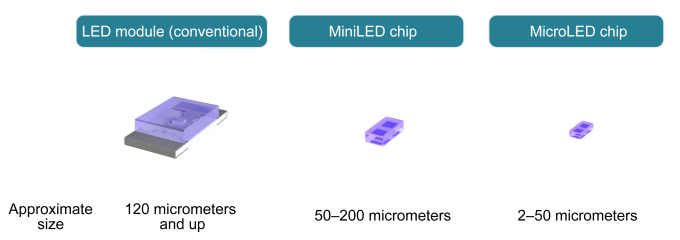
Micro LED chips are microscopic LED chips less than 0.1 millimeters in size. Display technology using these Micro LED chips takes smaller versions of the LEDs used as light sources in everyday lighting and traffic lights and arranges them across entire display panels. This allows displays to leverage LED’s characteristics of high brightness, low power consumption, and long lifespans while using the small LED chips to create detailed images.
Micro LED displays produce rich, painting-like images by precisely controlling the color and brightness of each pixel. This technology is based on the same principle behind the large screens seen in sports stadiums. But Micro LED displays use smaller individual light sources to produce highly detailed images viewable from a close distance. A Micro LED chip is less than half the size of a standard LED, and some are less than 1/6 of the size.
As the technology evolves, Micro LEDs are being considered for use in a wide range of devices such as digital signage, televisions, wearable devices, and augmented reality (AR) smart glasses. By enabling smaller and more sophisticated displays, Micro LED technology has the potential to contribute to significant advances in electronic devices.
Challenges for practical application of Micro LED displays
There are, however, multiple obstacles to the widespread use of Micro LED displays.
One such obstacle is cost. The price tags of about 80,000 USD on an 89-inch display and about 150,000 USD on a 110-inch display launched in 2022 illustrate this. As of January 2024, a major South Korean electronics manufacturer sells Micro LED displays for TVs but the prices are still higher than the price range for the average consumer. The cost of the Micro LED chips themselves is one factor in the high prices, but it is thought that the lack of an established, efficient manufacturing process is also a factor. This may mean that manufacturing costs have not been reduced as much as expected.
Another big challenge is the LED arrangement process (mass transfer). When manufacturing a Micro LED display, more than 24 million red, green, and blue LED elements are necessary to form the more than 8 million pixels for a 4K display. A method called “pick and place” is used to position these LED elements on the circuit board. An elastomer stamp is used to pick up LED chips and transport them to the target location. There is a limit to the number of LED chips that can be moved at once, resulting in the problem of extremely long times required to move all of the chips.
Another bottleneck in the manufacturing process is low illumination rate and the repair of non-illuminating parts. The LED chips used to produce high-resolution images are so small that connection to the circuit board becomes difficult, leading to an increased trend in non-illumination. When an LED chip fails to illuminate, it leads to a pixel defect where it cannot show the correct color, or in the worst case a dead pixel. A partial repair is necessary to address the issue.
To take on these challenges, various manufacturers are developing assembly process technologies such as batch formation of LEDs on wafers and mass transfer of LED chips. Many other manufacturing approaches are also being tried. One is “tiling,” which arranges small LED displays like tiles to create one large display. Others involve sealing or laminating LED chips.
ArrayFIX can solve Micro LED display challenges
As Micro LED display technology continues to evolve, Dexerials provides products that can play important roles in Micro LED display manufacturing. In addition to products such as optical films and optical elastic resins, Anisotropic Conductive Film (ACF) is drawing attention as an indispensable part of electrically connecting various parts of the display. In particular, a particle-arrayed ACF called ArrayFIX was developed for the miniaturization of terminal connections such as those found on Micro LED chips, and its potential applications have been highly evaluated.
ArrayFIX technology for Micro LEDs
As the connection area between LED chips and substrate shrinks in the Micro LED display manufacturing process, ArrayFIX continues to evolve to meet that challenge. Specifically, the diameter of conductive particles is smaller than in previous products, resulting in higher particle density that enables greater precision in positioning.
Previously, the highest density ArrayFIX ACF had a particle diameter of 3.2 micrometers and a particle density of 28 kpcs/mm2, designed for Chip on Glass (COG) technology to mount ICs for high-resolution displays such as those for smartphones. However, ArrayFIX for Micro LEDs requires even higher precision, so we are designing a version with particle diameter reduced to 2.2 micrometers and particle density increased to 58 kpcs/mm2.
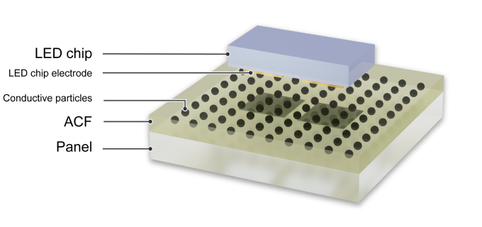
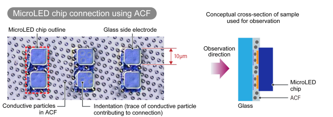
ArrayFIX for Micro LEDs enables stable connections due to the arrayed particles and low-resistance connection to extremely small electrodes of 100 μm² and below. Additionally, because the particles maintain their positions, excellent insulation is provided even with extremely small distances between electrodes.
The use of ArrayFIX can simplify the manufacturing process by enabling processing at lower temperatures than those required for conventional solder bonding and removing the need for Au/Sn bump formation. Simply applying ACF to the substrate is all the preparation that is required. With less pre-processing needed compared to other bonding methods, significant time and cost savings can be expected. In addition, temporary fixing of LEDs during mass transfer is possible between room temperature and 50°C, followed by thermocompression bonding all at once later. This can increase the efficiency of large-scale display manufacturing.
Innovative ACF placement technology for Micro LED display manufacturing
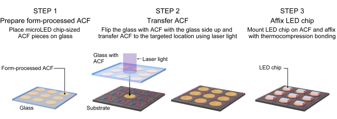
High-precision chip mounting is a critical factor in the Micro LED display manufacturing process, significantly influencing the final product’s quality. To take on this challenge, Dexerials has developed an innovative way to accurately place Pre-Cut ACF pieces in targeted locations. The key to this technology is micron-sized pieces of ArrayFIX. To be specific, we devised technology to use lasers to transfer ACF only to places where mounting is required. This allows ACF placement only where it is needed to enable high-precision mounting of LED chips on the circuit board.
Other applications of this technology are also possible. We are considering a process to remove a specific LED chip and the ACF around it with a laser, transfer a new ACF piece to a targeted location, and repeat bonding. This has the potential to improve display quality and manufacturing efficiency. In addition, this technology can make it possible to transfer ACF to only the substrate connection area. We are also exploring further applications such as the manufacturing of transparent Micro LED displays.
By leveraging these cutting-edge technologies, will continue its technological development efforts to bring richness and convenience to everyone’s lives.
From smartphones and tablets to TVs and computers, thin displays have become integral to our modern lives.
The display technology has undergone an impressive evolution. ACF has been fundamental to advancing display technologies, from LCD to OLED and flexible OLED. Let’s explore how display technology has evolved and examine ACF’s vital contribution to this journey.
The development of liquid crystal displays (LCDs) and the contribution of ACF
The LCD story began in the 1960s with a breakthrough discovery: liquid crystals could be used to create visual displays.
This technology found its first commercial applications in calculators and wristwatches during the 1970s, before expanding to larger formats like laptops, TVs, and monitors in the 1990s.
In LCD’s evolution, the push toward thinner profiles and higher resolutions was paramount.
ACF proved instrumental in this development by providing reliable circuit connections.
The technology delivers not only ultra-thin connections but also ensures robust bonding, exceptional reliability, and effective electrical isolation between adjacent circuits.
Its versatility extends to various substrates, enabling connections for Tape Carrier Package (TCP) and Chip on Film (COF) package signal outputs to displays, while also supporting Chip on Glass (COG) driver IC implementation.
The adoption of ACF has enabled higher resolutions through the miniaturization of circuits and contributed to thinner and lighter devices through the miniaturization of driver ICs.
LCD technology has developed rapidly since the discovery of the principles behind the use of liquid crystals for visual display. but it may not have been possible to achieve the modern thin and high-resolution displays without the evolution of ACF technology.
The emergence of OLED displays and the adaptation of ACF technology
As LCD technology matured, OLED emerged as the next generation of display technology.
After the Eastman Kodak Company announced the fundamental principles behind OLED in 1987, elements that emit their own light were used to achieve display technology that featured higher contrast than conventional LCD, wide viewing angles, thinness, and lightweight.
However, initial adoption was hampered by manufacturing costs and technical hurdles. Several factors contributed to OLED’s initially slow market penetration: prohibitive production costs, limited lifespan of blue organic electroluminescent elements, and image retention issues with static content.
Additionally, the complexity of OLED manufacturing processes and low yield rates presented significant challenges for mass production.
OLED technology made its breakthrough in the late 2000s, first appearing in small displays for smartphones and digital cameras as manufacturers overcame initial technical hurdles.
As the technology’s advantages became increasingly apparent, OLED displays expanded into large-screen TVs and flexible displays. Throughout this evolution, ACF technology adapted and advanced to accommodate OLED’s unique electrical properties and circuit designs.
Flexible OLED and ACF’s technical innovation: achieving Flex on Plastic (FOP) and Chip on Plastic (COP)
The advent of flexible OLED displays, utilizing polyimide substrates, marked a breakthrough in creating durable, highly flexible foldable displays.
While this technology opened new possibilities for flexible displays and wearable devices, it presented a significant challenge: maintaining reliable electrical connectivity with flexible substrates.
To address this challenge, innovative mounting technologies emerged, including FOP (mounting flexible FPC directly On Plastic) and COP (mounting hard IC On plastic substrate).
These solutions rely heavily on ACF technology to create secure connections between flexible plastic substrates and rigid driver ICs. ArrayFIX, represents a significant advance in this field. This particle-arrayed ACF technology delivers exceptional connection reliability in an extremely small area while maintaining electrical isolation between adjacent electrodes. By ensuring precise, dependable connections even in challenging environments, ArrayFIX has dramatically enhanced flexible OLED performance.
ACF’s technical features and its contributions to display technology
ACF technology stands as a cornerstone in advancing high-definition display technologies across LCD, OLED, and flexible OLED platforms. Its distinctive capabilities include ultra-fine pitch connections at pitches below 100 micrometers and remarkable adaptability to various electrode materials.
This versatility in accommodating different conducting materials, from ITO electrodes to metal electrode, has been instrumental in pushing the boundaries of display resolution and performance across all display technologies. The innovative ArrayFIX technology showcases the continued evolution of ACF. Its precise particle alignment capability enables optimized connections for specific electrode materials and pitches, driving further improvements in display performance. The technology’s success with both FOP and COP applications has made it essential for the advancement of flexible OLED technology.
ACF will support the display technology of tomorrow
Throughout the display industry’s evolution from LCD to OLED and flexible OLED, ACF has been a crucial enabler of technological progress.
Its contributions have been fundamental to achieving higher resolution displays, enhanced designs, and reliable connectivity solutions. Looking ahead, it remains committed to advancing ACF technology to support emerging display technologies such as microLED and silicon OLED, continuing our mission to enhance products that enrich our daily lives.
Anisotropic Conductive Film (ACF) serves as an adhesive for securing and electrically connecting electronic components, like integrated circuits (ICs), to circuit boards.
Originally introduced in 1977, ACF is now a staple in nearly all digital devices that employ flat panel displays—think smartphones, tablets, and high-definition TVs.
ACFs are typically used to connect the display panel to the flexible substrate that transmits signals to the panel or to the IC. Common applications of ACF include: COG (Chip-on-Glass), which connects the IC and glass substrate FOG (Flex-on-Glass), which connects the flexible substrate and glass substrate FOB (Flex-on-Board), which connects the flexible substrate and rigid substrate Other applications of ACF extend to smart cards, camera modules for CCDs (charge-coupled devices), and CMOSs (complementary metal oxide semiconductors). Shenzhen olian design and manufactur all the COG,COF,COP,FOG,FOB,FOP,FOF,TFOG,TFOF ACF bonding machines.
How ACFs can bond, conduct, and insulate
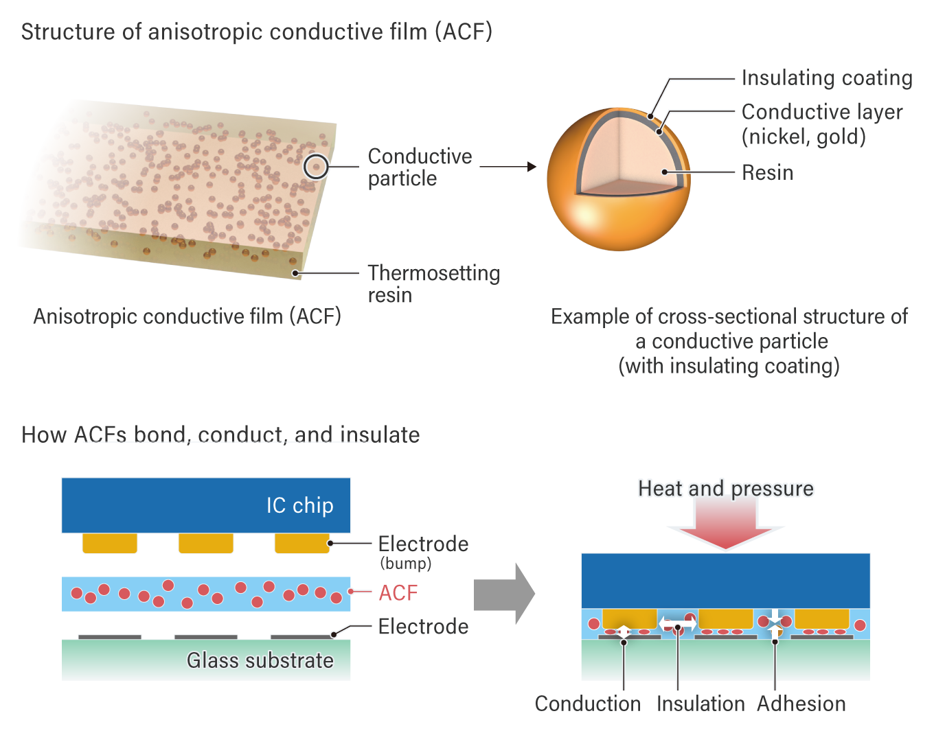
Anisotropic Conductive Film serves three primary functions simultaneously: adhesion, electrical conduction, and insulation. This unique capability allows manufacturers to connect a large number of pads at once.
Unlike traditional soldering, ACF enables fine pitch connections. The film is composed of conductive particles dispersed in a thermoset resin. A typical particle features a polymer core coated with nickel or gold, covered by an insulating layer.
When heat and pressure are applied, the opposing pads capture these particles. This process breaks the insulating coating to establish a vertical electrical connection. Particles trapped between pads remain insulated, preventing short circuits.
Key Technical Specifications:
Bonding Temperature: Ranges from 110°C to 180°C.
Film Thickness: Available from 10 to 45μm.
Film Width: Ranges from 0.5 to 20mm.
Roll Length: Available from 10 to 300m.
The ACF structure and bonding process
The bonding process is precise and efficient. Shenzhen Olian recommends following these steps for optimal results:
Clean the surface of the board to be attached.
Apply heat and pressure to the ACF with the release liner attached.
Peel off the release film carefully.
Align the pads of the IC chip to the ACF.
Apply heat and pressure again to finalize the bond.
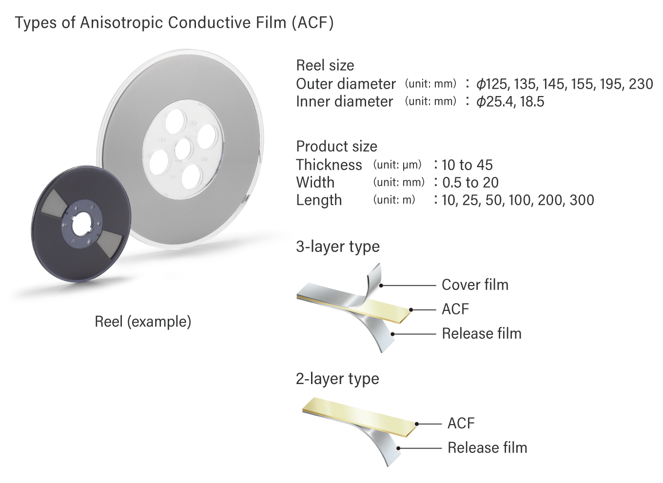
ACFs are sold in reels, as shown in the photo below. They come in a wide range of film thicknesses. From 10 to 45μm, widths from 0.5 to 20mm, and lengths from 10 to 300m.
The figure below illustrates two types of ACFs: a three-layer type, where ACF is sandwiched between a protective film and a release film.
And a two-layer type where only the release film is used. Each type offers different benefits. The three-layer type reduces the risk of dust contamination, while the two-layer type eliminates the need to remove the protective film during bonding.
The advantages of bonding components with ACFs
As technology advances each year, circuit boards are becoming increasingly fine pitch, the area of connecting pads is shrinking, and the spacing between them is narrowing.
While reflow soldering and connector components are traditionally used for bonding electronic components such as ICs to circuit boards, ACFs provide a solution to these trends.
However, a disadvantage of ACF is that it is challenging to bond components of different shapes simultaneously, which is common in reflow soldering.
Also, since ACF is an adhesive, it cannot be freely removed and reattached like mechanical connectors.
Why Choose ACF?
Benefits of ACF
Can bond components on glass substrates
Enables batch connections of multiple pads
Enables fine pitch connections
Pb-free
Quick bonding at relatively low temperatures
Thinner bonding area
The history of ACF and its innovation
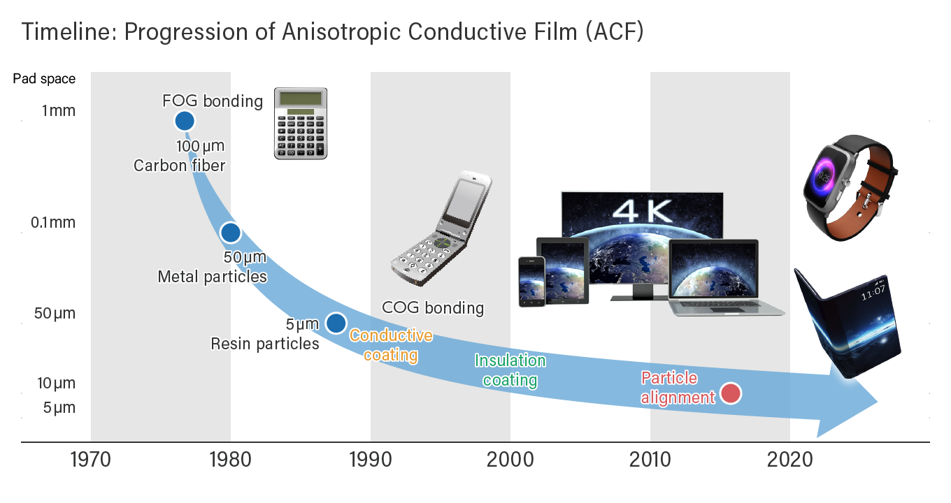
Dexerials has been continually enhancing ACF since its introduction in 1977. Initially, the conductive particles used were carbon fiber and solder particles. However, in 1988, Dexerials developed particles plated with nickel and gold.
By the 1990s, Dexerials had successfully developed a technology to coat the surface with insulating material.
As digital devices have evolved towards higher definition, Dexerials has adapted to the trend of fine pitch connections by reducing the particle size from 5μm to 2.8μm.
In 2014, Dexerials developed a technology to uniformly align conductive particles in thermosetting resin.
And in 2016, began marketing the product as “particle-arrayed Anisotropic Conductive Film” (ArrayFIX). This product contributes to the miniaturization, slimming design of digital devices, and higher resolution displays.
Selecting the best type of ACF
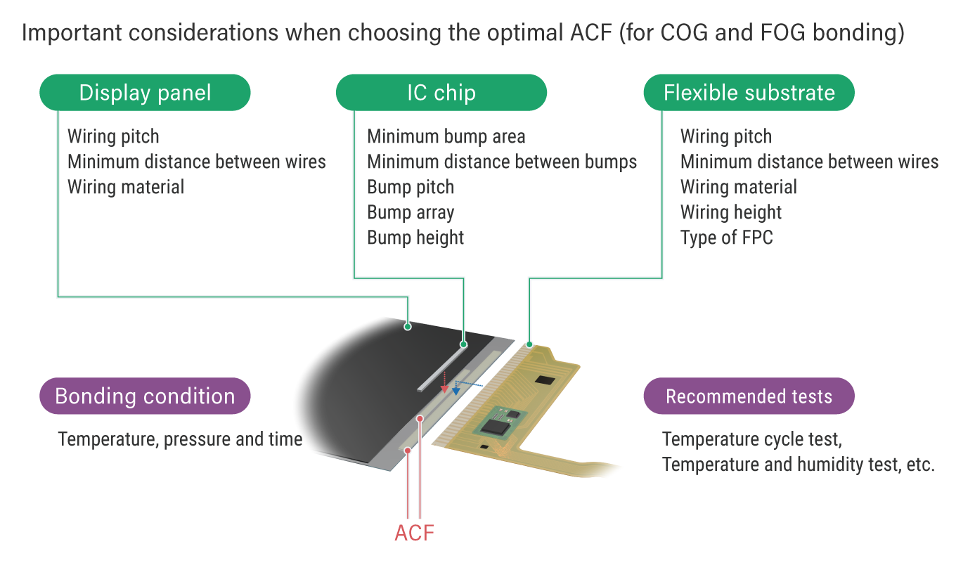
When selecting the best ACF, several factors should be considered, including the type of adherend, connection area, distance between pads, height of pads, and heat resistance.
ACF is composed of either epoxy resin or acrylic resin that cures with heat. we recommends acrylic ACF for applications where Flexible Printed Circuits (FPCs) and substrates (PCBs or glass substrates) are to be bonded, and where the design is intended to be reworked after the main bonding. (Please note that Dexerials does not recommend reworking itself. Dexerials advises that rework should only be done after reliability evaluations have been conducted to ensure that there are no issues.) Dexerials does not recommend ACF with epoxy resin if there is a possibility that the customer will rework. The primary reason is that it often damages the substrate to be reworked. This is because cured epoxy resin does not dissolve in solvents, and the process involves scraping off the residue.
Reworking after bonding typically involves heating the bonding area with a heat gun, hot iron, hot plate, etc., and then peeling off the FPC. Afterward, the cured resin residue between the pads on the board should be carefully removed using a solvent such as Methyl Ethyl Ketone (MEK) or N-Methyl-2-pyrrolidone (NMP) and a cotton swab. However, Dexerials does not recommend reusing FPCs because FPCs often curl during the peeling process and cleaning the resin residue between the pads on the FPC side is challenging.
With over 40 years of leadership in ACF technology, Dexerials can provide services including the initial setup, proposing an appropriate ACF, and post-connection analysis and evaluation. If you have any questions about ACF application, please feel free to contact us.
About Shenzhen Olian
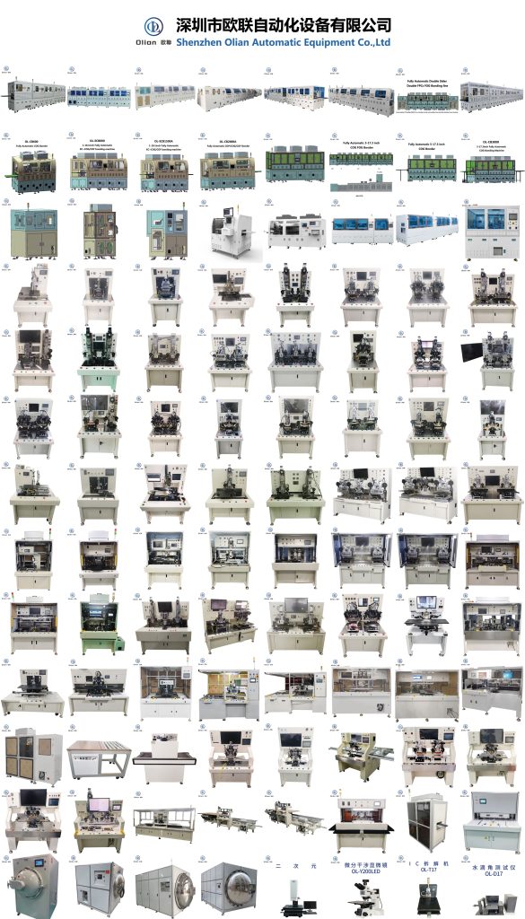
Shenzhen Olian Automatic Equipment Co., Ltd ,established in 2012, is a national high-tech enterprise specializing in the research and development, sales, production, and service of automation equipment for FPD flat panel displays and new flexible screen displays. The company holds multiple invention patents, utility model patents, and software copyrights. At present, the company has a professional R&D team of more than 100 workers, as well as a professional team for production management, quality management, and after-sales service.
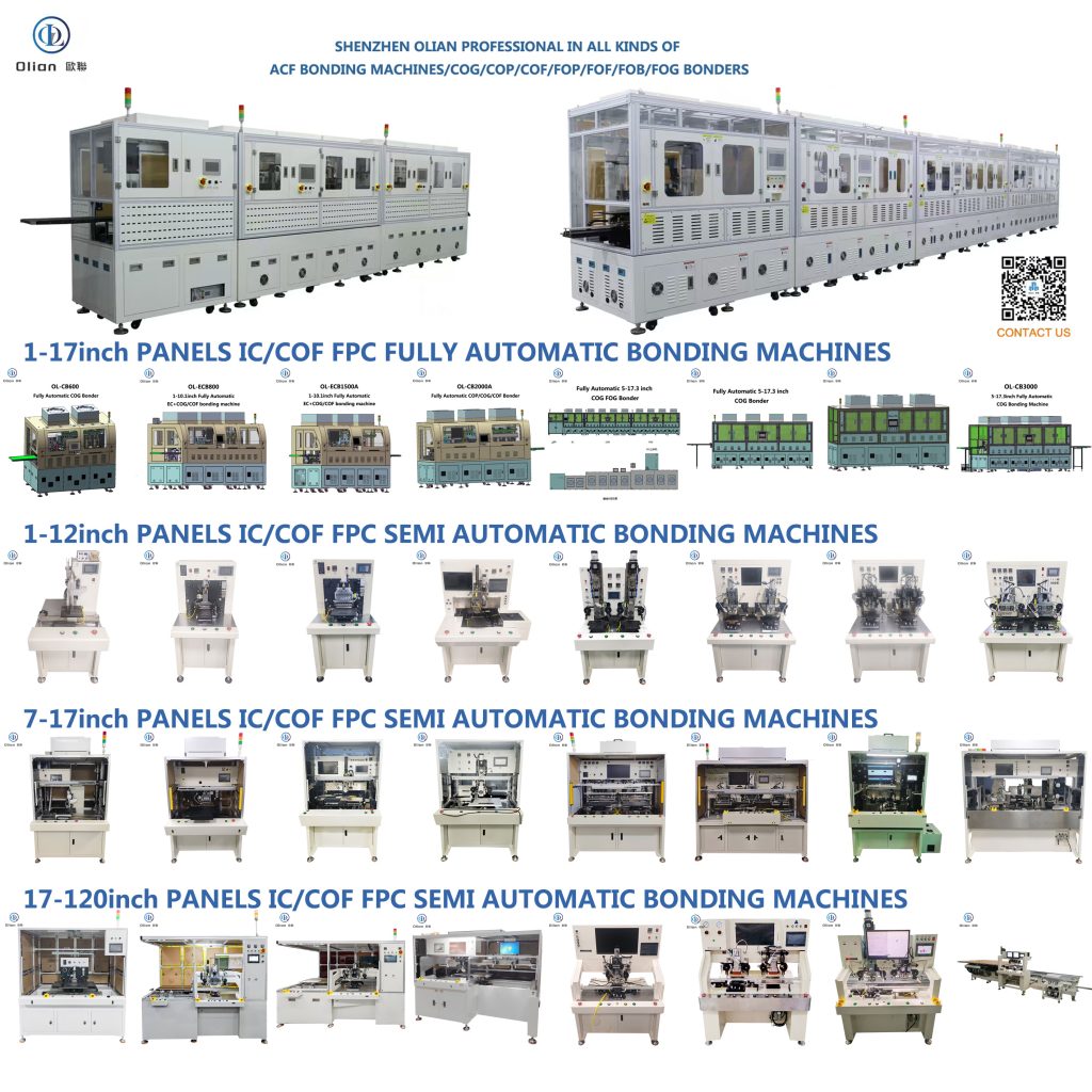
Olian’s products include LCM module factories and full process equipment (COG COF COP ,FOG FOB FOF FOP FOC TFOG TFOF bonding, AOI, dispensing, backlighting, soldering), achieving manufacturing of integrated display and touch products. The company’s series of products are widely used in display fields such as mobile phones, electronic tags, tablets, smart wearables, automotive displays, televisions, computers, etc., and provide overall solutions for smart factories.
ACF Bonding Machine Manufacturer for LCD Display Production
Discover how ACF bonding machines drive LCD/OLED/MINI LED/Microled/COP… display production — from COG/COF/COP/FOG/FOB/FOP/FOF/OLB bonding processes to choosing the right manufacturer. Explore bonding-machine.com for industry-leading solutions, technical specifications, and expert guidance on anisotropic conductive film bonding equipment.
ACF Bonding Machine Manufacturer for LCD Display Production: The Complete Guide to Choosing the Right Equipment
📌 Quick Navigation
What Is ACF Bonding and Why Does It Matter?
The Critical Role of ACF Bonding Machines in LCD Display Production
Types of ACF Bonding Processes: COG, COF, FOG Explained
Key Technical Specifications to Evaluate
How to Choose the Right ACF Bonding Machine Manufacturer
bonding-machine.com: Your Trusted ACF Bonding Equipment Partner
Industry Trends & Future Outlook
Frequently Asked Questions (FAQ)
What Is ACF Bonding and Why Does It Matter?
In the world of LCD and OLED display manufacturing, there’s a microscopic process that makes every screen you use possible — ACF bonding.
ACF stands for Anisotropic Conductive Film — a specialized adhesive material that conducts electricity vertically (through its thickness) while remaining electrically insulating horizontally (across its surface). Originally developed by Sony Chemical (now Dexerials) in 1977, ACF has become the indispensable “neural synapse” of modern display panels, enabling electrical connections between driver ICs, flexible printed circuits (FPCs), and glass substrates at pitches as fine as 30 micrometers or below.
Think of it this way: within an area roughly the size of a fingernail, hundreds of electrical contacts must be simultaneously connected with micron-level precision — that’s exactly what ACF bonding achieves. Without this technology, the smartphones, tablets, laptops, televisions, automotive displays, and industrial HMI screens we rely on every day simply couldn’t exist.
And the machine that makes this process happen? That’s the ACF bonding machine — the precision equipment that applies temperature, pressure, and alignment control to create reliable, repeatable electrical interconnections using ACF material.
The Critical Role of ACF Bonding Machines in LCD Display Production
LCD display production is a multi-stage manufacturing process where the bonding stage is arguably the most precision-demanding step. Here’s where ACF bonding machines fit in the production flow:
LCD Module Assembly Process Flow
Stage
Process
Equipment Category
1
Glass substrate cleaning
Cleaning equipment
2
ACF film lamination (attach ACF to glass)
ACF bonding machine (lamination unit)
3
Driver IC bonding (COG — Chip on Glass)
ACF bonding machine (COG bonder)
4
FPC bonding (FOG — Film/FPC on Glass)
ACF bonding machine (FOG bonder)
5
Protective sealing (silicone dispensing)
Dispensing equipment
6
Light-shielding tape application
Tape attaching equipment
7
Backlight unit (BLU) assembly
BLU assembly equipment
8
Final inspection & testing
Inspection equipment
As the table shows, ACF bonding machines are involved in at least 2–3 critical stages of LCD module assembly. The quality of bonding directly determines:
✅ Display image stability — no flickering, line defects, or dead pixels
✅ Signal transmission reliability — consistent electrical conductivity at every contact point
✅ Product lifespan — resistance to thermal cycling, mechanical stress, and environmental aging
✅ Yield rate — reducing rework and scrap directly improves production economics
A single bonding defect — a misaligned IC, insufficient ACF compression, or a trapped particle short — can render an entire display panel defective. This makes the choice of ACF bonding machine manufacturer a strategic production decision, not merely a procurement task.
Types of ACF Bonding Processes: COG, COF, FOG Explained
Understanding the different bonding configurations is essential when selecting equipment. Here’s a detailed breakdown:
1. COG (Chip on Glass) Bonding
COG bonding attaches a bare driver IC chip directly onto the ITO (Indium Tin Oxide) electrode pads on the LCD glass substrate using ACF as the interconnect medium.
Process Steps:
ACF film is laminated onto the glass bonding area
The driver IC is aligned to the glass electrode pads using a high-precision vision alignment system
Pre-bonding (temporary attach) with low pressure
Main bonding with controlled temperature (typically 180–220°C), pressure (typically 15–30 MPa), and time (typically 8–15 seconds)
ACF resin thermosets, conductive particles are compressed to form vertical electrical pathways
Key Challenges:
Pin pitch down to 30 μm or finer requires sub-micron alignment accuracy
Uneven pressure distribution causes connection reliability issues
Thermal management must prevent glass substrate stress
2. COF (Chip on Film/FPC) Bonding
COF bonding mounts the driver IC onto a flexible printed circuit (FPC) film first, then the COF package is bonded to the glass substrate. This configuration is increasingly preferred for:
High-resolution displays with narrow bezels
Foldable/flexible OLED displays
Displays requiring bendable interconnects
Advantages over COG:
The IC can be bent around the display edge → narrower bezel
Better thermal dissipation through the FPC substrate
Easier repair — the entire COF module can be replaced
3. FOG (FPC on Glass) Bonding
FOG bonding connects the flexible printed circuit board (FPC) to the glass substrate terminal area. This is the signal bridge between the display panel and the external system (motherboard, T-CON board, etc.).
Process Flow (after COG is completed):
Glass terminal area is cleaned
ACF is laminated onto the glass bonding pads
FPC is aligned to the glass pads
Pre-bond → Main bond (thermocompression)
FOG is often the final electrical interconnection step before the LCD module enters final assembly and testing.
Comparison Table: COG vs COF vs FOG
Parameter
COG
COF
FOG
Bonded Component
Bare IC chip
IC-on-FPC package
FPC alone
Bonded To
Glass substrate
Glass substrate
Glass substrate
Bezel Impact
Wider (IC on surface)
Narrower (IC bends around edge)
Minimal (FPC at edge)
Pin Pitch
Finest (down to ~30 μm)
Fine (~40–60 μm)
Moderate (~80–150 μm)
Alignment Accuracy Required
±2–5 μm
±2–5 μm
±15–30 μm
Typical Applications
Standard LCDs, TN/STN
High-res LCD, OLED, foldable
All LCD/OLED modules
Repairability
Difficult (direct on glass)
Moderate (replace COF module)
Moderate
Equipment Needed
COG bonding machine
COF bonding machine
FOG bonding machine
Key Technical Specifications to Evaluate
When comparing ACF bonding machines from different manufacturers, these are the non-negotiable specifications that determine production capability:
🔧 Alignment Accuracy
Grade
Alignment Accuracy
Suitable For
Standard
±15 μm
FOG bonding, moderate-pitch applications
High-Precision
±5 μm
COF bonding, fine-pitch LCD/OLED
Ultra-High-Precision
±2 μm or better
COG bonding, finest pitch ICs
Tip from bonding-machine.com: Always verify alignment accuracy under actual production conditions (not just laboratory specs). Request a live demonstration with your specific product dimensions.
🌡️ Temperature Control
Temperature range: Typically 100–280°C
Temperature uniformity across bonding head: ±2°C or better
Ramp-up speed: Fast heating reduces process time and ACF pre-curing risk
Temperature measurement: Thermocouple embedded in bonding tool vs. infrared sensing
Precision temperature control is critical because ACF’s conductive particles must be compressed at the exact thermosetting temperature — too hot causes ACF degradation, too cold means incomplete curing and unreliable connections.
💪 Pressure Control
Pressure range: 2–5 MPa (adjustable for different ACF types and substrates)
Pressure uniformity: ±5% or better across bonding area
Parallelism of bonding head: Critical for uniform particle compression
Force measurement: Load cell-based real-time monitoring preferred
⏱️ Process Time & throughput
Single bond cycle time: 6–20 seconds (main bond)
UPH (Units Per Hour): Ranges from 300 to 1,200+ depending on machine configuration
Pre-bond + Main-bond sequential time: Total cycle including alignment, pre-bond, main-bond, and cooling
👁️ Vision Alignment System
The vision system is the “eyes” of the bonding machine. Key parameters:
Camera resolution: Minimum 2 megapixels; 5+ MP for ultra-fine pitch
Magnification: Adjustable (typically 2x–10x)
Alignment mark recognition: Support for multiple mark types (cross, circle, L-shape, custom)
💡 A machine that costs 20% more but delivers 3% higher yield can save hundreds of thousands of dollars annually on a high-volume production line.
Shenzhen Olian(bonding-machine.com): Your Trusted ACF Bonding Equipment Partner
At Shenzhen olian (bonding-machine.com), we understand that ACF bonding isn’t just a mechanical process — it’s the heart of display manufacturing. Our commitment goes beyond selling machines; we deliver complete bonding solutions.
What Sets bonding-machine.com Apart
🎯 Comprehensive Product Line
We offer ACF bonding machines covering the full spectrum of display production needs:
±15 μm alignment, high throughput, multi-FPC bonding capability
ACF-L Series
ACF Lamination
Pre-bond ACF attachment, high accuracy film positioning
Multi Series
Multi-function
COG+FOG or COF+FOG combined, flexible production line configuration
🔬 Deep Process Expertise
We don’t just deliver hardware. Our team of process engineers provides:
ACF bonding recipe development — optimized temperature/pressure/time parameters for specific ACF materials (Dexerials, Resonac, Hitachi Chemicals, and Chinese domestic ACF brands)
New product introduction (NPI) support — from first article bonding through production qualification
Yield improvement consulting — systematic defect analysis and process optimization
🌍 Global Service Network
Fast response: 24/7 remote technical support
On-site service: Engineers available for installation, training, and troubleshooting
Regional offices: Service hubs in key display manufacturing regions
Spare parts: Local inventory for critical components
🏭 Proven Track Record
Our machines are running in production lines at display manufacturers serving:
Smartphone and tablet LCD/OLED panels
Automotive infotainment and instrument cluster displays
Industrial HMI and medical display modules
Television and large-format display panels
Wearable and IoT device displays
Industry Trends & Future Outlook
The ACF bonding equipment industry is evolving rapidly alongside display technology advances. Here are the key trends shaping the future:
1. Finer Pitch, Higher Precision
As display resolutions increase (4K, 8K, and beyond), driver IC pin pitches continue shrinking. The industry is moving from 40 μm pitch toward 20 μm and below, requiring bonding machines with:
Alignment accuracy of ±2 μm or better
Higher-resolution vision systems (8+ MP cameras)
More sophisticated alignment algorithms with AI-assisted pattern recognition
2. Foldable & Flexible Display Bonding
Foldable OLED displays (used in smartphones and emerging foldable laptops) demand:
COF bonding as the primary configuration
Bonding machines capable of handling ultra-thin flexible substrates
Specialized ACF materials with enhanced bend reliability
New process parameters for flexible substrate bonding (lower temperature to protect flexible materials)
3. Mini LED & Micro LED Backlight Bonding
Mini LED and Micro LED displays require mass transfer bonding — connecting thousands of tiny LED chips to the substrate. This creates demand for:
High-speed multi-head bonding machines
Gang bonding (simultaneous bonding of multiple chips)
Specialized ACF or alternative interconnect materials
4. Automation & Smart Manufacturing
Industry 4.0 integration in bonding equipment includes:
MES (Manufacturing Execution System) connectivity — real-time production data upload
SPC (Statistical Process Control) — automatic monitoring of bonding parameters
Predictive maintenance — AI-based analysis of machine health data
Digital twin — virtual machine models for process simulation and optimization
5. Domestic ACF Material Adoption
With China now the world’s largest LCD panel producer, domestic ACF material suppliers are rapidly gaining market share (domestic ACF adoption rate has risen to approximately 25%). Bonding machines must be compatible with:
Both Japanese premium ACF (Dexerials, Resonac) and Chinese domestic alternatives
Different ACF specifications (thickness, particle size, curing temperature)
Flexible recipe management for quick material changeover
Frequently Asked Questions (FAQ)
Q1: What is the difference between ACF bonding and soldering?
A: ACF bonding uses anisotropic conductive film adhesive to create electrical connections through thermocompression, while soldering uses molten metal alloy. ACF bonding offers several advantages for display production:
Lower processing temperature (180–220°C vs. 250+°C for soldering)
No flux residues that could contaminate the display
Simultaneous connection of hundreds of contacts in a single bonding cycle
Suitable for glass substrates that cannot tolerate soldering temperatures
Compatible with fine-pitch connections below 40 μm
Q2: How long does an ACF bonding machine typically last?
A: With proper maintenance, a quality ACF bonding machine has a service life of 8–10 years or more. Key longevity factors include:
Regular calibration (typically monthly)
Bonding head replacement schedule (every 6–12 months depending on usage)
Servo system maintenance
Software updates and alignment system recalibration
Q3: Can one machine handle both COG and FOG bonding?
A: Yes. Multi-function bonding machines(full automatic bonding line) can handle both COG and FOG bonding in a single platform, typically through:
Changeable bonding head tooling
Switchable vision system configurations
Adjustable pressure and temperature ranges
This is ideal for factories producing multiple product types with moderate throughput needs.
Q4: What ACF materials are compatible with bonding machines?
A: Modern ACF bonding machines from reputable manufacturers are designed to work with the full range of commercially available ACF films, including:
Dexerials (formerly Sony Chemical) — industry benchmark
Resonac (formerly Hitachi Chemical) — widely used in automotive and industrial displays
Chinese domestic brands — rapidly improving quality, cost-effective alternative
Compatibility depends on ACF thickness (typically 15–40 μm), particle type (nickel, gold-coated, solder), and curing temperature profile. At bonding-machine.com, we test and certify compatibility with major ACF suppliers.
Q5: What is the typical yield rate for ACF bonding?
A: With a properly calibrated machine and optimized process, ACF bonding yield rates typically reach 98–99.5% for standard products. Factors affecting yield include:
ACF material quality and storage conditions
Glass substrate cleanliness
Alignment accuracy and consistency
Pressure and temperature uniformity
Operator skill and process discipline
Our process engineers at bonding-machine.com routinely help customers achieve and maintain >99% yield.
Q6: How do I get a quotation for an ACF bonding machine?
A: Simply contact our team with your production requirements — we’ll provide a detailed quotation including:
Machine configuration recommendation
Process capability assessment for your specific product
Delivery timeline and installation plan
Training and after-sales support package
TCO analysis comparison
Conclusion: The Right Manufacturer Is Your Production Partner
Choosing an ACF bonding machine manufacturer for LCD display production isn’t a transactional purchase — it’s a strategic partnership that directly impacts your product quality, production yield, and competitive position in the display market.
The ideal manufacturer provides not just a machine, but a complete bonding solution: equipment designed for your specific process needs, deep technical expertise in ACF bonding chemistry and physics, responsive after-sales support, and continuous innovation to keep pace with display technology evolution.
At bonding-machine.com, that’s exactly what we deliver — from our comprehensive bonding machine lineup to our process engineering support and global service network.
The Ultimate Guide to Choosing the Right Bonding Machine for Your Display Production Line in 2026
In the fast-evolving world of consumer electronics, display quality can make or break your product. Whether you’re manufacturing smartphones, tablets, smartwatches, automotive dashboards, or large-format TVs, bonding machines are the unsung heroes ensuring precise, reliable connections between chips, films, and glass substrates.
At bonding-machine.com, we specialize in high-precision ACF, COF, COG, COP, FOG, FOB, and OLBbonding solutions that power modern display module assembly. If you’re looking to boost yield rates, reduce defects, and scale production efficiently, this guide will help you navigate the options.
What Is a Bonding Machine and Why Does It Matter?
Bonding machines use controlled heat, pressure, and anisotropic conductive film (ACF) to create electrical connections in LCD/OLED/Touch panel manufacturing. Key processes include: COG (Chip on Glass): Bonding driver ICs directly to glass substrates. COF (Chip on Film): Attaching chips to flexible circuits. FOG (Film on Glass): Connecting FPC to glass. FOB (Film on Board) and OLB (Outer Lead Bonding): Critical for larger panels and integrated modules.
These technologies are essential for high-resolution displays in mobile phones, wearables, laptops, and automotive applications. Poor bonding leads to defects like line mura, open circuits, or delamination—issues that hurt both quality and profitability.
Key Factors to Consider When Selecting a Bonding Machine
1.Panel Size Compatibility
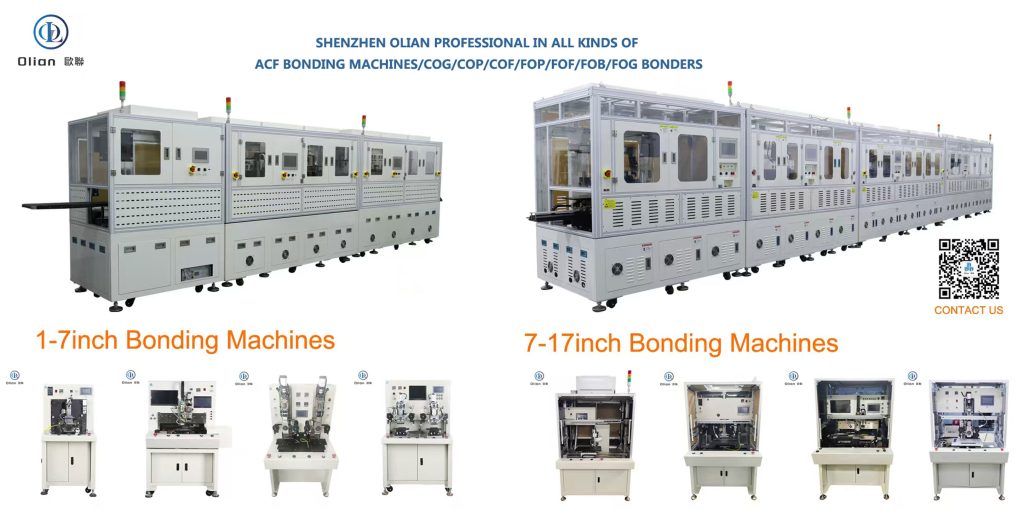
Choose machines matched to your production needs: 1-7 inch for small wearables and phones, 7-17 inch for mid-size tablets and monitors, or larger formats up to 85-120 inches for TVs and commercial displays.
2.Automation Level
Manual or semi-automatic systems suit prototyping and low-volume runs. Fully automatic lines with servo motors, vision alignment, and plasma cleaning deliver higher throughput and consistency for mass production.
3.Precision and Process Control
Look for pulse heating, multi-station designs, AOI integration, and accurate temperature/pressure control. These features minimize ACF bonding failures and support fine-pitch applications.
4.Throughput and Yield
High-speed models with pre-bonding and main-bonding stations can significantly improve your line efficiency.
5.Reliability and Support
Partner with experienced manufacturers who offer full-line solutions, training, and after-sales service. Olian has supplied equipment to leading brands including Huawei, BOE, BYD, Foxconn, and more.
Popular Bonding Machine Solutions from Olian
Small Size Series (1-7 inch): Ideal for smartphones and wearables. Models like the OL-F006 (dual station FOG) and OL-CB1000 (fully automatic COG/COF) deliver excellent precision in compact footprints.
Mid Size Series (7-17 inch): Versatile lines such as OL-3000 and OL-1100 support COG, COF, FOG, and FOB processes for tablets and automotive displays.
Large Format Solutions: 65-120 inch OLB and FOB bonders for TV and commercial panel production. Supporting Equipment: ACF attaching machines, plasma cleaners, AOI inspection systems, and full turnkey production lines.
All machines emphasize robust construction, easy maintenance, and integration into smart factory environments.
Benefits of Upgrading Your Bonding Equipment
–Higher first-pass yield and lower scrap rates –Faster cycle times and reduced labor costs –Better support for flexible and high-resolution displays (including foldables) –Compliance with stringent quality standards in automotive and medical electronics
Many manufacturers report significant ROI within months after switching to modern automated bonding systems.
Ready to Optimize Your Production?
Selecting the right bonding machine is a strategic investment in your display manufacturing future. Whether you’re scaling up a new line or upgrading existing equipment, expert guidance makes all the difference.
Visit bonding-machine.com today to explore our full product range, download specifications, or contact our engineering team for a customized solution. With years of expertise serving global display leaders, Olian is your trusted partner for precision bonding technology.
The touchscreen module is one of the most complex sub-assemblies in modern electronics. It brings together the cover glass, touch sensor, display panel, and flexible printed circuits (FPC) into a single unit that must deliver flawless optical clarity, responsive touch input, and long-term durability. Every layer in this stack must be bonded with micron-level accuracy, or the final product suffers from parallax errors, reduced brightness, touch drift, and premature failure.
For manufacturers producing capacitive touchscreens for smartphones, tablets, automotive displays, medical monitors, and industrial HMI panels, the bonding process is not a secondary step—it is the step that determines product quality. The best bonding machine for touchscreen module assembly must handle multiple bonding technologies within a single platform, from ACF thermocompression for electrical interconnects to OCA lamination for optical layer fusion.
Understanding the Bonding Technologies in Touchscreen Assembly
ACF Bonding for Electrical Interconnects
Anisotropic Conductive Film (ACF) bonding creates the electrical pathways between the touch sensor, driver IC, and FPC. In capacitive touchscreen modules, the touch controller IC is typically embedded on the FPC in close proximity to the sensor, and this FPC must be bonded to the glass substrate using ACF. The conductive particles in the ACF establish vertical conductivity while maintaining horizontal insulation, ensuring each trace connects precisely without shorting adjacent lines. After bonding, RTV silicone is commonly applied for electrical insulation and strain relief.
ACF Bonding Machine Manufacturer for LCD Displays
OCA Optical Bonding for Layer Lamination
Optically Clear Adhesive (OCA) bonding fuses the cover glass, touch sensor film, and display panel into a single optical unit. Unlike air-gap bonding, which uses perimeter adhesive and leaves an air cavity between layers, OCA bonding eliminates internal reflections and improves light transmission by over 90%. This results in better contrast, vivid colors, and superior sunlight readability—critical for outdoor and automotive applications. OCA is typically supplied as a pre-cut dry film sheet and applied through roll lamination followed by autoclave defoaming.
The advantages of OCA bonding extend beyond optical performance. It enhances structural integrity by bonding layers together as a solid mass, improving resistance to shock, vibration, and thermal cycling. It also prevents moisture and dust ingress between layers, which is essential for outdoor and industrial applications. For manufacturers, OCA bonding delivers a premium product feel that consumers associate with high-end devices.
Hybrid Bonding for High-Volume Production
Hybrid bonding combines the precision of OCA lamination with advanced vacuum pressing to achieve bubble-free results at production scale. In this process, OCA film is precisely positioned between layers, components are aligned under vacuum to eliminate trapped air, and controlled pressure and temperature complete the fusion. This method is increasingly used for high-volume smartphone and tablet manufacturing where throughput and first-pass yield must both exceed 95%.
What Makes the Best Bonding Machine for Touchscreen Module Assembly
Multi-Process Capability
The best bonding machine for touchscreen module assembly is not limited to a single bonding method. It integrates ACF thermocompression for FPC-to-glass interconnects and OCA roll lamination for sensor-to-cover-glass and display-to-sensor fusion. A unified platform reduces capital expenditure, minimizes floor space, and simplifies operator training.
Sub-Micron Alignment Accuracy
Touchscreen modules require bonding accuracy within ±1.5 to ±3 micrometers. This is achieved through high-resolution CCD or CMOS vision systems with pattern recognition, telecentric lenses, and coaxial LED illumination. Auto-focus and overlay comparison functions eliminate operator dependency and ensure repeatable results across thousands of units.
Closed-Loop Thermal and Pressure Control
Pulse heating technology with PID auto-tuning delivers temperature ramp-up from ambient to 180°C in 2–3 seconds, with stability within ±0.5°C. Servo-driven pressure systems with 0.1 N resolution apply force precisely across the bonding zone, while active gravity compensation prevents substrate warping. These controls are essential for preventing delamination, void formation, and thermal damage to sensitive components.
Cleanroom-Compatible Design
Touchscreen bonding must occur in controlled environments to prevent dust and debris from becoming trapped between optical layers. The best machines feature ISO Class 6 or better cleanroom compatibility, with enclosed bonding chambers, laminar airflow, and electrostatic discharge protection.
Flexible Panel Size Support
From 1-inch wearable displays to 27-inch tablet screens and beyond, the ideal bonding machine accommodates a wide range of panel sizes without mechanical retooling. Quick-change fixtures and programmable recipes allow seamless transitions between product variants.
Industry 4.0 Integration
Modern bonding machines offer Ethernet, USB, and RS-232 connectivity for MES integration, remote diagnostics, and real-time process monitoring. Recipe storage, SPC data output, and predictive maintenance alerts help manufacturers maintain Six Sigma quality levels while minimizing unplanned downtime.
Applications Across Industries
Consumer Electronics
Smartphones, tablets, and laptops demand ultra-thin bezels and high touch sensitivity. COF and FOG bonding technologies enable the flexible circuit routing needed for edge-to-edge displays, while full OCA lamination eliminates parallax and improves the premium feel users expect.
Automotive Displays
In-vehicle infotainment systems, digital instrument clusters, and rear-seat entertainment screens must operate reliably from -40°C to +85°C while resisting vibration and shock. OCA optical bonding enhances structural integrity and prevents moisture ingress, while ACF bonding ensures stable electrical connections under thermal cycling.
Medical and Industrial Equipment
Surgical monitors, patient monitoring systems, and industrial HMI panels require high optical clarity, glove-compatible touch response, and resistance to chemical disinfectants. Precision bonding ensures these displays maintain calibration accuracy and long-term reliability in demanding environments.
Repair and Refurbishment
Professional repair centers use bonding machines to fix delaminated touchscreens, replace damaged cover glass, and repair FPC interconnect failures. A versatile machine that handles both OCA re-lamination and ACF re-bonding maximizes service capability and return on investment.
How to Choose the Right Bonding Machine for Your Touchscreen Production
Define Your Product Range: Identify the panel sizes, bonding methods, and production volumes you need to support today and in the next three to five years.
Evaluate Bonding Accuracy Requirements: High-resolution displays (4K, 8K) and fine-pitch driver ICs demand ±1.5 µm or better alignment. Lower-resolution industrial panels may tolerate slightly wider tolerances.
Assess Throughput Needs: High-volume smartphone factories need fully automatic lines with robotic handling and inline AOI. Low-to-medium volume operations may prefer semi-automatic systems with manual loading but automatic alignment and bonding.
Consider Total Cost of Ownership: Factor in not just the purchase price, but also consumables (ACF tape, OCA film), maintenance schedules, spare parts availability, and technical support responsiveness.
Verify Supplier Credentials: Look for manufacturers with ISO 9001 certification, proven installations in your target industry, and references from brands you recognize. A supplier with in-house R&D and customization capability can adapt the machine to your specific process requirements.
Conclusion
The best bonding machine for touchscreen module assembly is one that unites precision, versatility, and reliability in a single platform. It must master ACF bonding for electrical interconnects and OCA lamination for optical layer fusion, delivering sub-micron accuracy at production speed. Whether you are scaling up smartphone manufacturing, producing ruggedized automotive displays, or operating a professional repair center, the right bonding equipment is the foundation of product quality and manufacturing efficiency.
As touchscreen technology evolves toward foldable displays, larger panels, and tighter integration with display drivers, the demands on bonding equipment will only increase. Partnering with an experienced manufacturer ensures your production capabilities keep pace with market expectations.
Ready to find the best bonding machine for your touchscreen module assembly line?
Explore our complete range of bonding solutions at bonding-machine.com and speak with our application engineers about your specific requirements.
Precision bonding starts with the right partner.welcome to Shenzhen Olian.
Touchscreen module assembly relies heavily on advanced bonding machines to establish reliable electrical and mechanical connections between the display panel, touch sensors, and driving circuits. These machines are essential for achieving the thin, high-performance, and durable designs required in modern consumer and industrial electronics.
Core Bonding Technologies in Touchscreen Assembly
Different bonding processes are utilized depending on the specific application, cost requirements, and design constraints:
COG (Chip on Glass): This process involves directly bonding the driver IC onto the glass substrate. It simplifies the module structure, reduces signal transmission links, and significantly lowers the overall screen thickness. It is widely used in LCDs and touchscreens for smartphones and tablets.
COF (Chip on Film): The driver IC is mounted directly onto a flexible FPC (Flexible Printed Circuit), which is then bonded to the glass. This method supports ultra-narrow bezel designs and provides excellent flexibility and signal transmission stability, making it ideal for high-end smartphones, automotive displays, and wearable devices.
FOG (FPC on Glass): This process bonds the flexible printed circuit (FPC) directly to the glass substrate. It is a critical step in connecting the touch or display module to the main control board.
COB (Chip on Board): The IC is bonded directly onto a rigid PCB. While this results in a slightly thicker module, it offers superior mechanical stability, easier maintenance, and lower manufacturing costs. It is commonly used in industrial control screens, POS machines, and large-format touch displays.
COP/FOP (Chip/FPC on Plastic): Emerging technologies designed specifically for next-generation flexible displays (such as foldable phones and smartwatches), allowing direct bonding onto plastic substrates to achieve true flexibility.
Key Features of Modern Bonding Equipment
To ensure high production yields and precise connections, modern touchscreen bonding machines are engineered with several advanced capabilities:
High-Precision Visual Alignment: Equipped with high-resolution CCD vision systems and nano-positioning platforms, these machines achieve micron-level alignment accuracy (often within ±3μm to ±5μm). This prevents defects like poor contact or virtual welding.
Advanced Thermal Compression: Machines utilize either constant temperature or pulse heating methods with specialized heating heads (made of tungsten steel, titanium alloy, etc.). They offer precise control over temperature, pressure, and time to ensure uniform bonding without damaging sensitive components.
Automated Process Integration: Fully automated production lines often integrate multiple steps, including plasma cleaning, ACF (Anisotropic Conductive Film) attachment, automatic bonding, and post-bonding Automated Optical Inspection (AOI) to detect misalignments or bubbles.
Intelligent Control Systems: Modern equipment uses PLC + HMI (Human-Machine Interface) control cores, allowing for easy parameter setting, real-time status monitoring, and automatic fault alarms to maintain stable mass production.
Typical Applications
Bonding machines are fundamental to the manufacturing of a wide range of display and touch products, including:
Consumer Electronics: Smartphones, tablets, laptops, and smartwatches.
Automotive Electronics: Curved dashboard displays and high-precision center control screens.
Automatic COF Bonding Machine for Display Panel Production
What Is an Automatic COF Bonding Machine?
An automatic COF (Chip on Film/chip on FPC) bonding machine is a precision assembly system that mounts driver ICs onto flexible polyimide film substrates OR FPC using Anisotropic Conductive Film (ACF) technology OR gold to gold technology.
Sometimes,bond the COF on the glass or on the PCB,we also call it COF bonding technology. But in fact ,they are differnet processes..
In shenzhen olian, we can do these both technology (Chip on Film/chip on FPC) and (ACF bonding /Gold to Gold Bonding).
chip on fpc bonding
Unlike manual or semi-automatic systems,
fully automatic COF bonders handle the entire process—from ACF attachment and IC placement to thermocompression bonding—without operator intervention. This makes them essential for high-volume display panel production where consistency, speed, and micron-level accuracy determine manufacturing yield.
COF bonding differs from COG (Chip on Glass) and COB (Chip on Board) in that the chip is mounted on a flexible film carrier rather than directly on glass or a rigid PCB.
This flexibility enables ultra-thin bezels, curved displays, and foldable screen designs that are now standard in smartphones, tablets, automotive dashboards, and premium TVs.
Why Automatic COF Bonding Matters in Modern Display Manufacturing
The global display industry is pushing toward higher resolutions, larger panel sizes, and more complex form factors. As panels evolve from HD to 4K, 8K, and beyond, the pitch between bonding pads shrinks dramatically—often to sub-10 micrometer levels. Manual alignment simply cannot achieve the repeatability required at these scales.
Automatic COF bonding machines solve this by integrating advanced vision systems, servo-driven motion platforms, and closed-loop thermal control.
The result is bonding accuracy within ±5 to ±15 micrometers, temperature stability within ±5°C, and cycle times under 4.5 seconds per bond—parameters that directly impact production capacity and return on investment.
For display panel manufacturers, the shift to automation is not merely about speed. It is about eliminating the variables that cause defects: misalignment, uneven pressure distribution, thermal drift, and human inconsistency.
In an industry where a single bonding defect can scrap an entire panel worth hundreds of dollars, automatic COF bonding is a risk mitigation strategy as much as a production tool.
Key Technical Specifications to Evaluate
When sourcing an automatic COF bonding machine for display panel production, these specifications separate professional-grade equipment from basic alternatives:
Alignment Accuracy
Look for sub-micron precision systems using CCD cameras with pattern recognition algorithms. Industry-leading machines achieve ±3 µm accuracy, which is necessary for 4K and 8K panel production where pad pitches are extremely fine.
Thermal Control System
Pulse heating technology with PID auto-tuning ensures rapid temperature ramp-up (180°C in 2–3 seconds) and stability within ±0.5°C to ±1°C.
The hot press head should use titanium alloy or molybdenum with surface flatness of 0.001 mm to guarantee uniform heat transfer across the bonding zone.
Pressure Control
Closed-loop servo pressure systems with 0.1 N resolution and 2 ms response time allow precise force application.
The pressure range should span from 0.1 N for delicate components up to 50 N or more for larger driver ICs, with active gravity compensation to prevent substrate deformation.
Vision System
High-resolution CCD or CMOS cameras (12 MP or higher) with telecentric lenses, coaxial and side LED illumination, and AI edge detection enable repeatable alignment to 3 µm. Auto-focus and overlay comparison features further reduce operator dependency.
Cycle Time and Throughput
Automatic systems should achieve cycle times under 30 seconds per bond, with production rates of 100+ units per hour for TAB bonding and 2,500+ pieces per day for repair applications. Multi-station configurations can further increase throughput by processing multiple bonds simultaneously.
Software and Connectivity
Modern machines feature intuitive touch-screen HMIs with recipe storage, error logging, and SPC (Statistical Process Control) output. Ethernet, USB, and RS-232 connectivity enable remote monitoring, firmware updates, and MES integration—critical for Industry 4.0 environments.
Applications Across the Display Industry
Automatic COF bonding machines serve diverse segments of the display ecosystem:
Smartphone and Tablet Manufacturing
The demand for bezel-less designs and foldable screens makes COF bonding the preferred method for connecting driver ICs to OLED and flexible LCD panels. The flexible film substrate allows the IC to be bent behind the display, maximizing active screen area.
Large-Format TV and Monitor Production
Machines supporting panels from 7 inches up to 100 inches or more handle everything from laptop screens to massive TV open-cell repairs. High-precision bonding ensures uniform image quality across the entire display surface.
Automotive Display Modules
Vehicle displays require extreme reliability under harsh temperature and vibration conditions. Automatic COF bonding delivers the consistent joint quality needed for automotive-grade displays, including curved instrument clusters and center-console screens.
Industrial and Medical Displays
Ruggedized displays for industrial control panels and medical diagnostic equipment benefit from the precision and repeatability of automatic bonding, where failure is not an option.
Repair and Refurbishment Centers
Professional LCD/LED TV repair facilities use automatic COF bonders to fix vertical lines, horizontal bands, black screens, and other common panel defects caused by failed driver IC connections. A single machine can handle panels from 15 inches to 120 inches, making it a versatile investment for repair businesses.
Industry Trends Shaping COF Bonding Technology
Integration with AI and Machine Learning
Next-generation bonding machines incorporate AI-driven predictive maintenance that forecasts heater life up to 200 cycles in advance, scheduling maintenance before quality degradation occurs. Machine learning algorithms also optimize bonding parameters in real time based on feedback from vision systems and thermal sensors.
Support for Advanced Packaging
The rise of heterogeneous integration, wafer-level packaging (WLP), and system-in-package (SiP) solutions is driving demand for COF bonders capable of sub-10 µm pitch bonding. Manufacturers are developing “one-stop” machines that handle multiple materials in a single pass, reducing thermal deformation and improving overall yield.
Sustainability and Energy Efficiency
European and North American markets increasingly prioritize energy-efficient equipment that reduces cycle time and waste. Modern pulse heating systems minimize power consumption by delivering heat only during the bonding phase, with rapid cooling to prevent thermal stress on surrounding components.
Multi-Station and Fully Automatic Production Lines
The industry is moving beyond single-station machines toward fully automated production lines with multi-station processing. These systems perform simultaneous COB and COF operations, robotic substrate handling, and inline AOI (Automated Optical Inspection) to achieve throughput rates suitable for mass production environments.
Choosing the Right Automatic COF Bonding Machine
Selecting equipment for your display panel production line requires balancing technical capability, production volume, and total cost of ownership. Consider these factors:
Panel Size Range: Ensure the machine supports your current and projected panel sizes, from small wearable displays to large-format TV panels.
Bonding Accuracy Requirements: 4K and 8K production demands ±5 µm or better accuracy. HD and lower-resolution applications may tolerate slightly wider tolerances.
Production Volume: High-volume factories need fully automatic lines with robotic handling, while repair centers may prefer compact single-station units with manual platform adjustment.
After-Sales Support: Look for manufacturers offering comprehensive training, spare parts availability, remote diagnostics, and on-site technical support. A one-year warranty is standard, but lifetime technical support adds significant long-term value.
Integration Capability: Confirm compatibility with your existing MES, quality management systems, and cleanroom requirements (ISO 6 recommended for precision bonding).
Conclusion
Automatic COF bonding machines are the backbone of modern display panel production, enabling the precision, speed, and reliability required by today’s high-resolution screens and advanced form factors.
Whether you are scaling up smartphone OLED manufacturing, producing automotive display modules, or operating a professional TV repair center, investing in the right automatic COF bonding equipment directly impacts your yield rates, operational costs, and competitive position.
As the display industry continues its shift toward foldable devices, larger panels, and smarter manufacturing, partnering with an experienced bonding machine manufacturer ensures you stay ahead of technological curves rather than struggling to catch up.
Ready to upgrade your display panel production capabilities? Explore our full range of automatic COF bonding machines at bonding-machine.com and connect with our engineering team for a customized solution tailored to your specific requirements.
Precision bonding starts with the right partner. Shenzhen Olian welcome you .
Leading ACF Bonding Machine Manufacturer for LCD Displays
Leading ACF Bonding Machine Manufacturer for LCD Displays
What Is ACF Bonding and Why It Matters for LCD Displays
Anisotropic Conductive Film (ACF) bonding is a key process in assembling and repairing LCD, OLED, and other flat panel displays. It uses a specialized adhesive film containing conductive particles to create reliable electrical connections under controlled heat, pressure, and time—without short-circuiting adjacent traces.
This technology is essential for processes such as:
COG (Chip on Glass)
COF (Chip on Film)
FOG (Film on Glass)
FOB (Film on Board)
TAB/OLB and more
Manufacturers and repair professionals searching for reliable ACF bonding machines for LCD displays need equipment that offers precision alignment, stable temperature control, and high throughput for both production lines and after-sales service.
Why Choose Olian as Your ACF Bonding Machine Manufacturer?
With years of expertise, Olian stands out among global suppliers by offering a comprehensive range of bonding equipment tailored to LCD display production and repair. Their machines support screen sizes from 1 inch wearables to large-format panels (up to 120 inches), making them ideal for mobile phones, tablets, automotive displays, TVs, laptops, and industrial applications.
Precision Servo Control & Pulse Heating
Ensures uniform pressure and temperature for defect-free bonds.
Advanced Alignment Systems
Dual-lens or high-resolution cameras for accurate positioning.
Versatile Models
From compact single-station units (e.g., OL-C012, OL-F003) to fully automatic production lines (e.g., OL-1500, OL-3000 series) for 1-7 inch and 7-17 inch panels.
Supporting Equipment
Including ACF attaching machines (OL-A0156, OL-A003), plasma ITO cleaners, COF punching machines, and AOI inspection systems for complete LCM module lines.
Reliability & Efficiency
Designed for high-volume manufacturing with options for multi-station, servo-driven, and pulse-heat configurations.
Olian’s equipment is widely used by leading brands and has supported over 2,600 companies, including partnerships with industry giants like Huawei, BOE, CSOT, Foxconn, TCL, and more.
Applications Across Industries
Whether you operate a display module factory, a professional LCD/LED TV repair center, or an automotive display assembly line, Olian’s ACF bonding solutions for LCD displays deliver consistent results. Their machines handle everything from small smartwatch panels to large TV open-cell repairs, helping reduce defects, improve yield rates, and lower operational costs.
What Buyers Look For: Key Considerations
Professionals searching for “ACF bonding machine manufacturer for LCD displays,” “COF FOG bonding machine,” or “LCD panel repair bonder” often prioritize:
Reliable manufacturers with proven track records
Machines offering pulse heat technology and servo control
Full production line solutions rather than standalone units
Strong after-sales support and customization options
Olian addresses these needs directly through their dedicated platform at bonding-machine.com, where you can explore detailed product specifications, videos, and contact options.
Partner with a Proven Manufacturer Today
As the display industry shifts toward higher resolutions, flexible panels, and smarter integration, having a dependable ACF bonding machine manufacturer becomes a strategic advantage. Olian combines advanced engineering, extensive industry experience, and customer-focused innovation to support your success.
Contact Olian today for tailored recommendations on ACF bonding machines for your LCD display production or repair needs. Visit bonding-machine.com or reach out directly to discuss your requirements with their expert team.