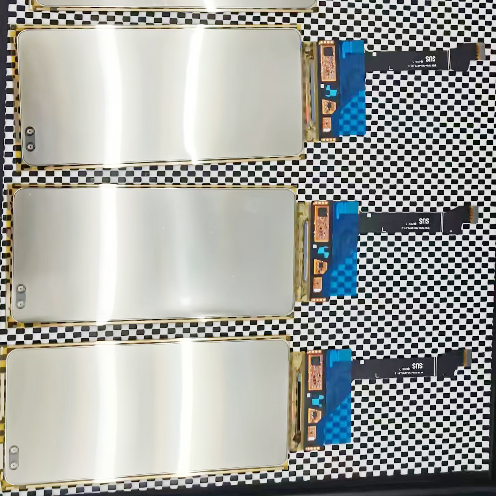
Before detailing the manufacturing workflow, it is crucial to clarify a fundamental technical distinction: AMOLED (Active-Matrix Organic Light-Emitting Diode) is a self-emissive display technology. Unlike LCDs, AMOLED screens do not require a backlight unit (BLU). Therefore, there is no “backlight assembly” step in this process. The complete production workflow is divided into four primary stages: Array, OLED Evaporation, Encapsulation, and Module Assembly.
This stage focuses on fabricating the driving circuits on a flexible substrate to provide precise electrical signals to each pixel.
This is the core stage where organic light-emitting materials are precisely deposited into pixels under high vacuum.
Since organic materials are highly sensitive to moisture and oxygen, this stage provides a protective shield.
This stage integrates the bare panel into a fully functional display module. It is the most complex phase involving precision mechanical and chemical processes.
A. Polarizer Attachment
A Circular Polarizer (CPL) is laminated onto the panel to absorb ambient light reflections, significantly enhancing contrast and outdoor visibility.
B. Precision Bonding Process (IC & FPC)
https://youtu.be/E4lvebUM_n0?is=WRQZASOtBLC9vNrj
This step establishes the electrical connection between the display panel and external control systems.
C. Dispensing & Sealing Process
To protect vulnerable bonding areas and enhance structural integrity:
D. Touch Integration & Optical Lamination
Modern flexible AMOLEDs utilize On-Cell or In-Cell technology, integrating touch sensors directly into the panel or encapsulation layer.
E. Structural Assembly
Double-sided tapes, foam pads, or metal brackets are applied to secure the module within the device’s frame, providing necessary cushioning for flexible bending zones.
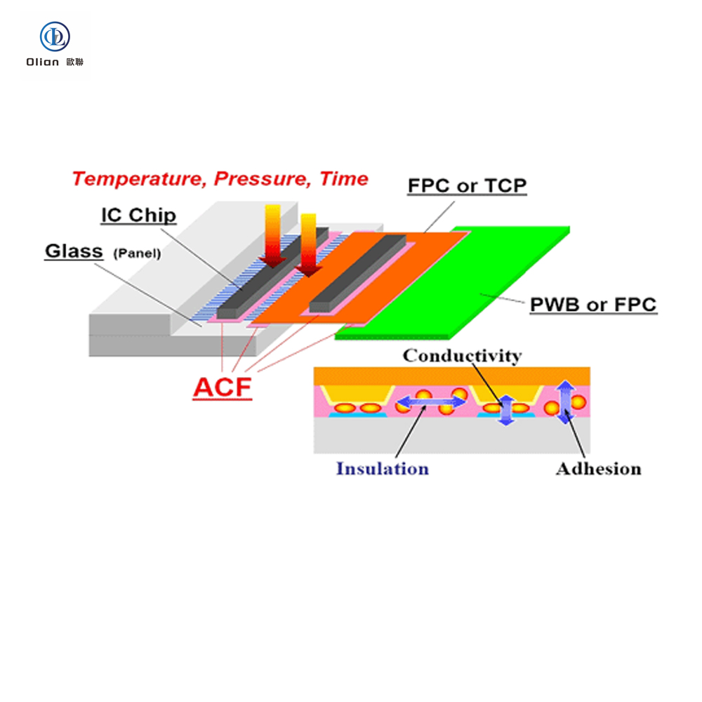
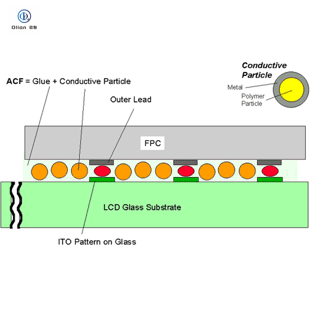
Anisotropic Conductive Film (ACF) is a specialized adhesive material. It contains conductive particles within an insulating resin. This unique structure allows vertical electrical conductivity. Simultaneously, it maintains horizontal insulation between circuits. ACF is essential for modern flat panel displays. It connects delicate components without short circuits. The film provides both adhesion and conduction. This dual function is critical for reliability. Olian Automatic utilizes this advanced material effectively. Our processes optimize the ACF performance. This ensures long-lasting display connections.
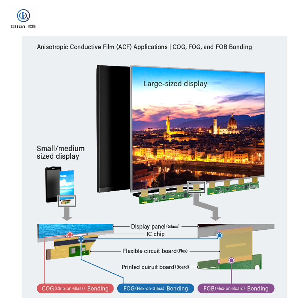
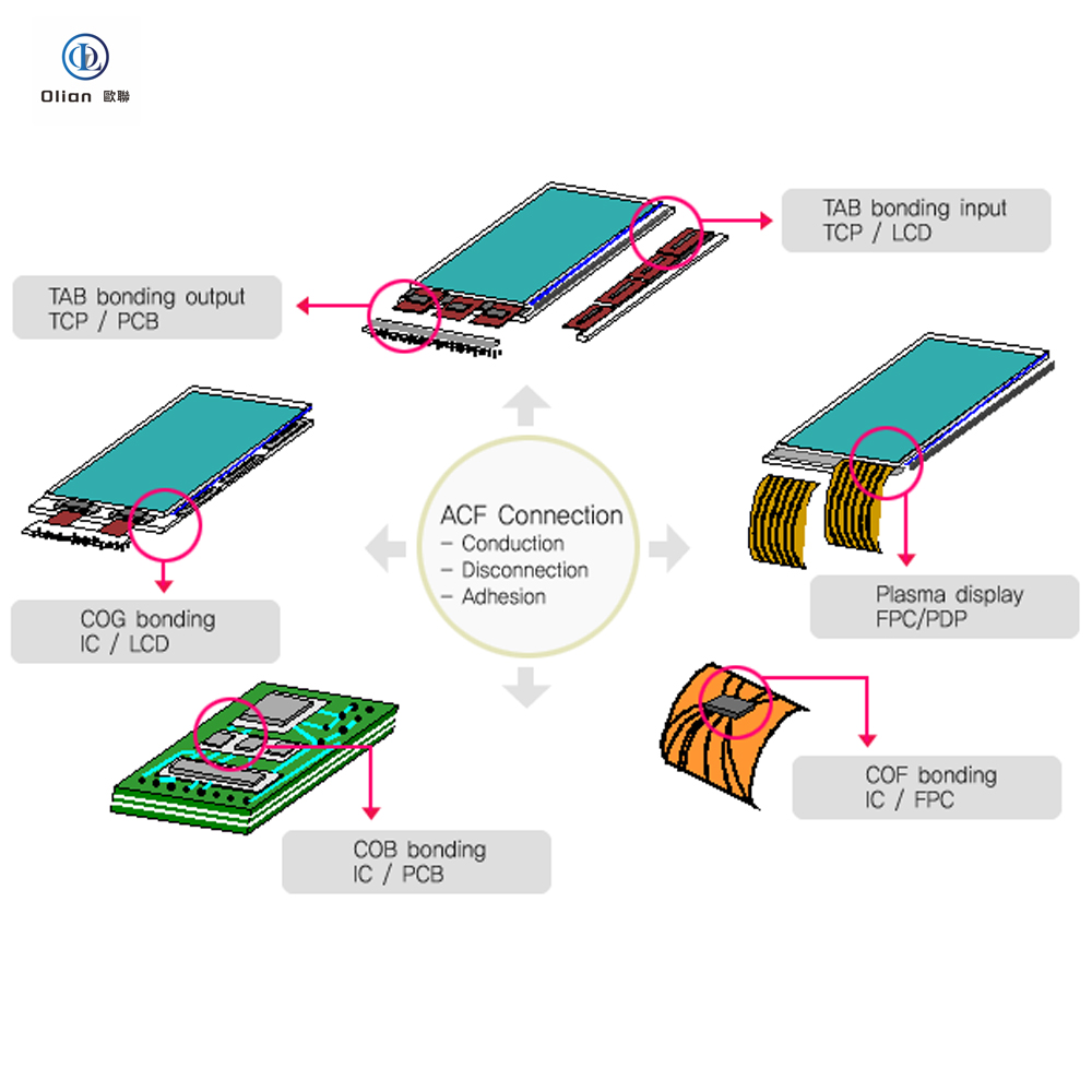
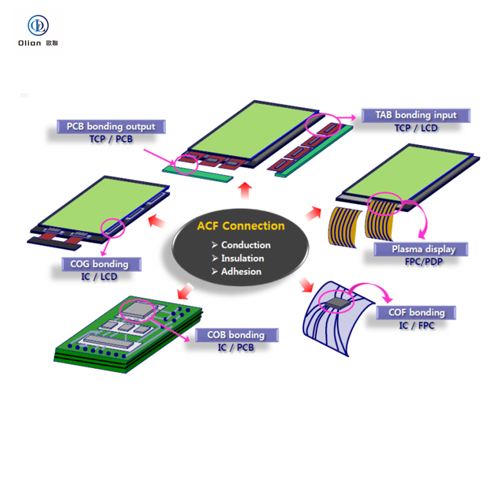
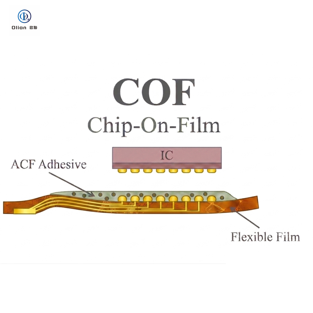
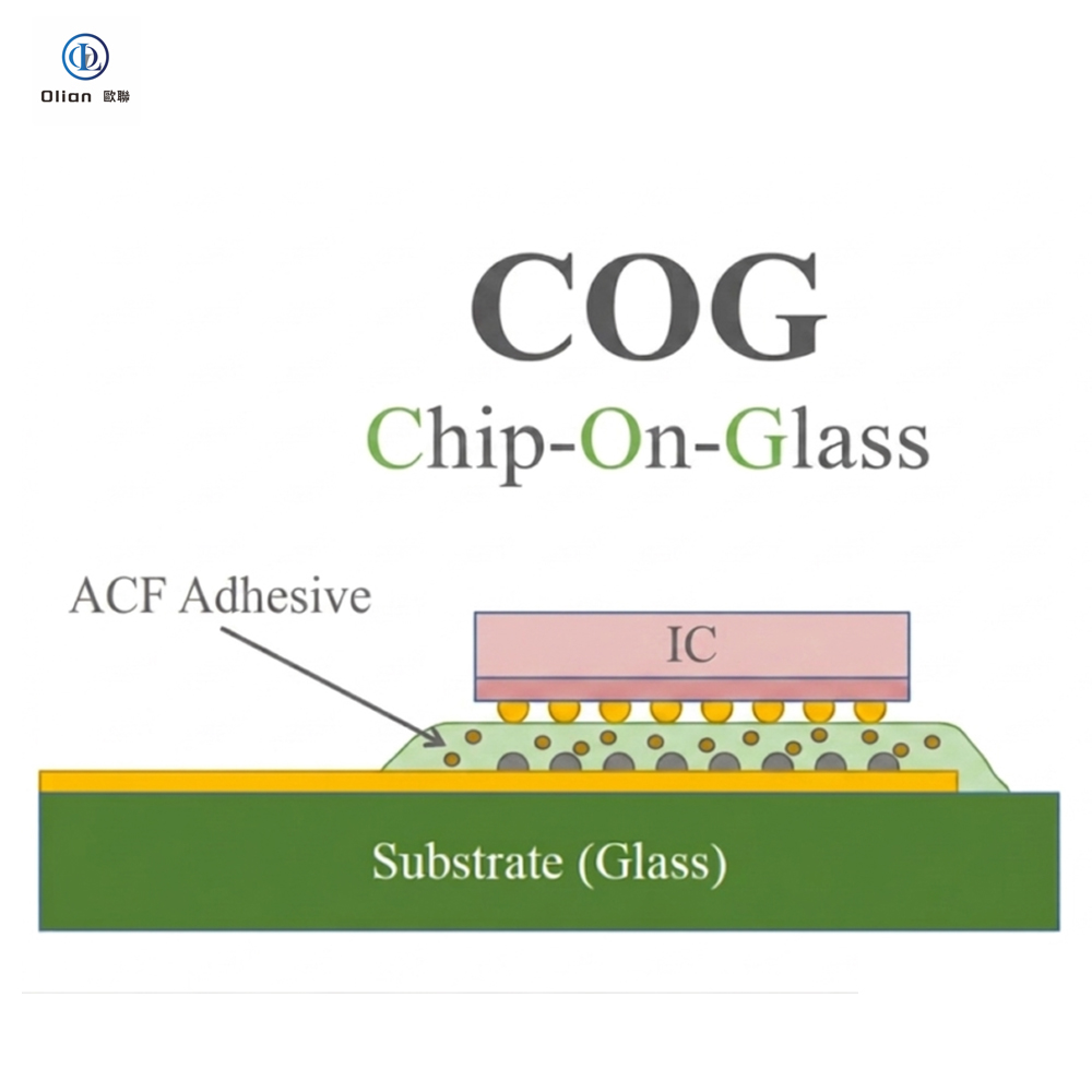
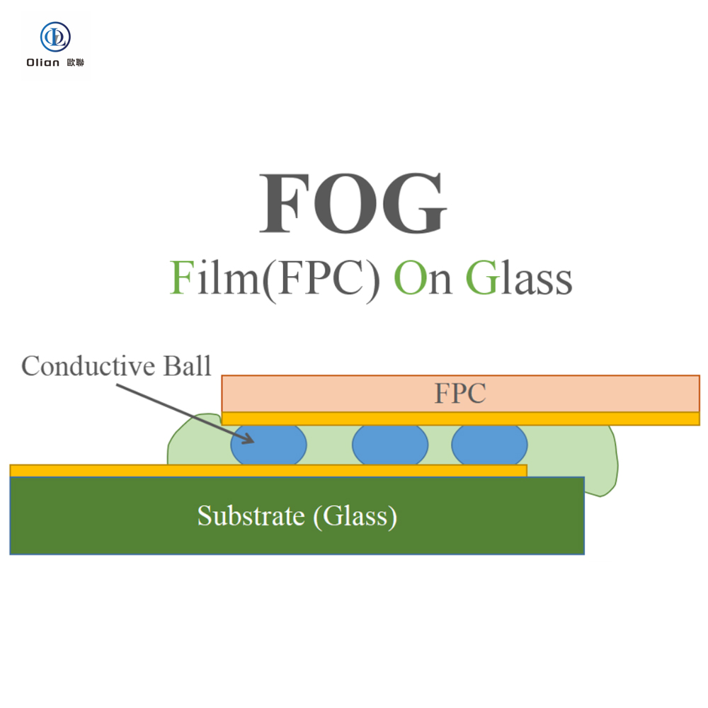
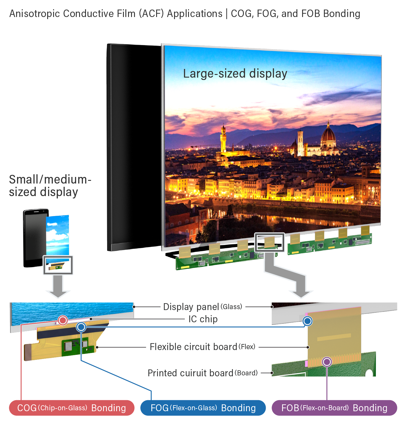
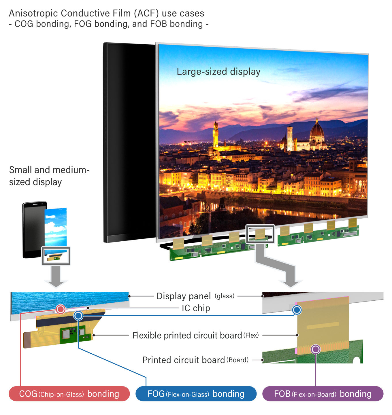
Several key bonding methods use ACF technology. Chip-on-Glass (COG) bonds IC chips directly to glass panels. This is common in LCD manufacturing. Chip-on-Film (COF) connects ICs to flexible circuits. This allows for thinner display bezels. Flex-on-Glass (FOG) attaches flexible boards to glass substrates. Flex-on-Board (FOB) connects flex circuits to rigid PCBs. Tape Automated Bonding (TAB) links TCP tapes to displays. Each process requires specific parameters. Olian Automatic masters all these techniques. We provide versatile solutions for various needs.
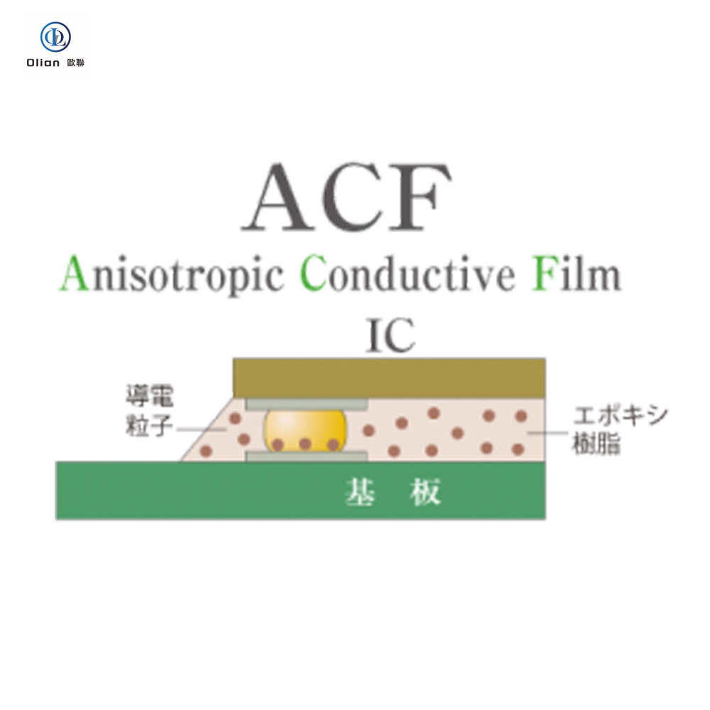
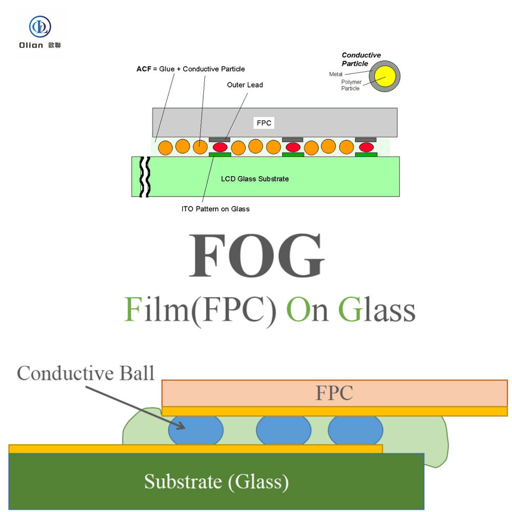
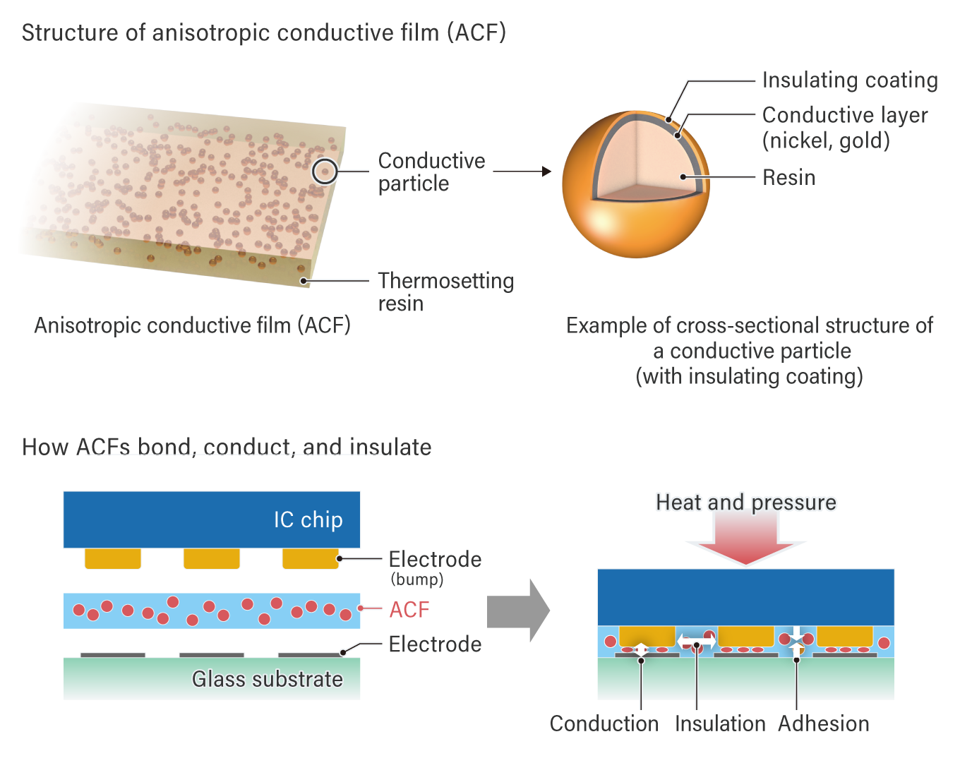
ACF stands for Anisotropic Conductive Film. It is a specialized adhesive material used in display assembly. The film contains conductive particles trapped in an insulating resin. It provides electrical conductivity in the vertical direction only. Simultaneously, it ensures electrical insulation in the horizontal direction. This unique property prevents short circuits between fine pitches. ACF also offers strong adhesion between components. It is the core material for COG, COF, and FOG bonding.
COG stands for Chip-on-Glass bonding. This process connects an IC chip directly onto a glass substrate. It is widely used in LCD and OLED panel manufacturing. The method eliminates the need for intermediate flexible tapes. COG bonding saves space and reduces module thickness. It requires precise alignment and controlled heat pressure. ACF is typically used as the interconnect material. This technique is common for source and gate driver ICs.
COF stands for Chip-on-Film bonding. This technique mounts IC chips directly onto a flexible film. The film is usually a Tape Carrier Package (TCP). COF allows for very narrow display bezels. It enables the bending of the film under the panel. This creates a “bottom bezel” free design. The flexible circuit connects the glass to the main PCB. It supports high-resolution displays with many signal lines.
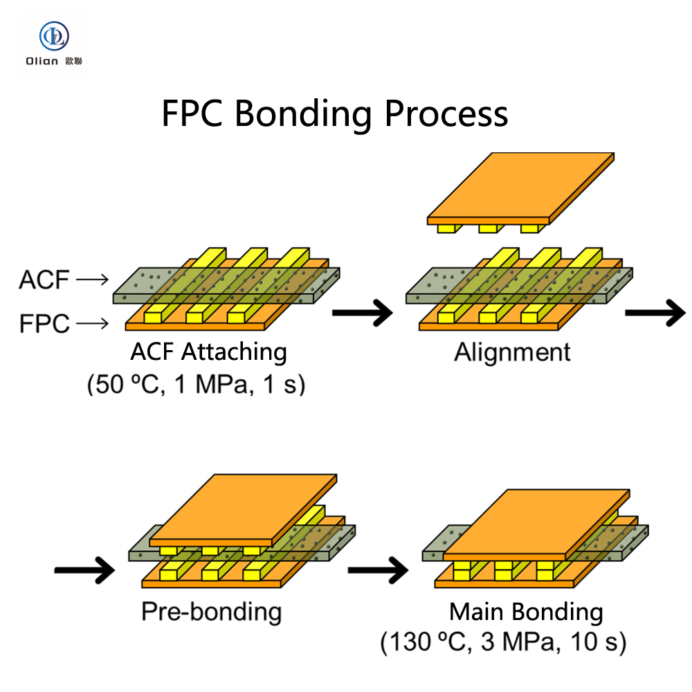
FOG stands for Flex-on-Glass bonding. This process attaches a Flexible Printed Circuit (FPC) to a glass panel. It serves as the interface between the rigid glass and external electronics. FOG bonding is essential for transmitting signals to the display. It uses ACF to ensure reliable electrical connection. The process requires high precision to align fine circuit traces. It is a standard step in LCD module assembly.
FOB stands for Flex-on-Board bonding. This method connects a flexible circuit (FPC) to a rigid Printed Wiring Board (PWB). It bridges the gap between flexible and rigid electronics. FOB is often used in the final assembly stage. It links the display module to the main system board. The connection must withstand mechanical stress and bending. ACF provides both electrical continuity and mechanical strength.
COP stands for Chip-on-Plastic bonding. Although less prominent in the diagrams, it is listed in the text. This technology bonds IC chips directly onto plastic substrates. It is increasingly used in flexible OLED displays. COP allows the entire display to be bendable or foldable. It replaces glass with polyimide or similar plastics. The bonding process requires lower temperatures to protect the plastic.
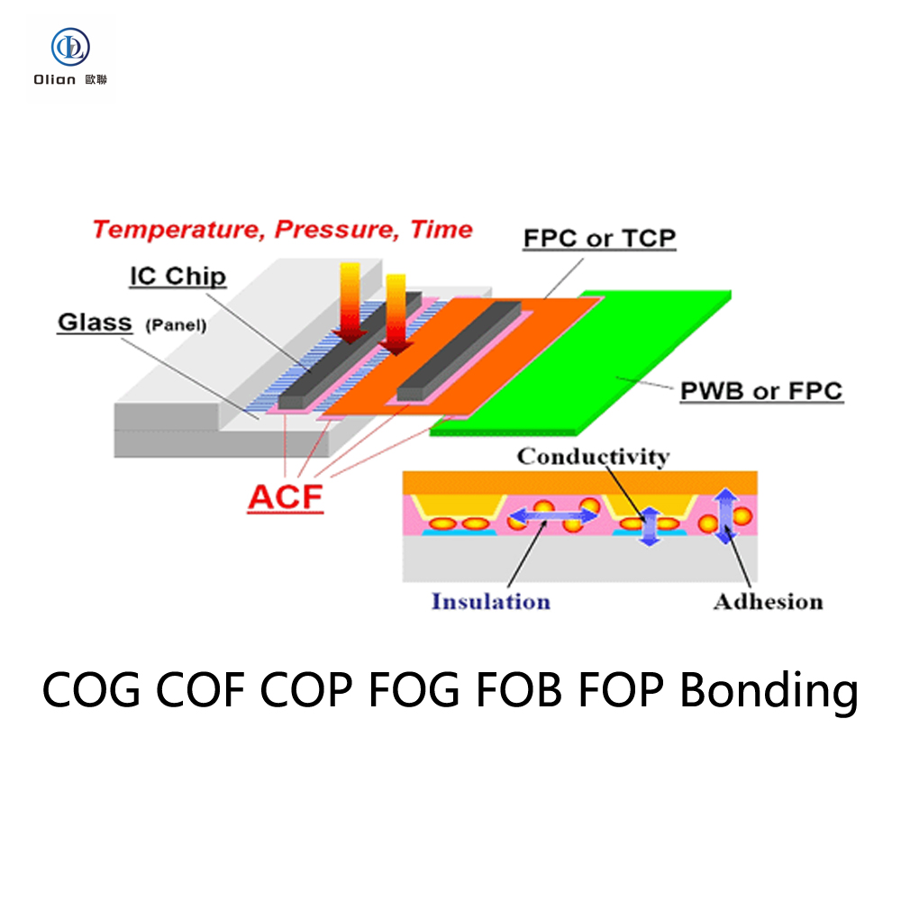
TCP refers to Tape Carrier Package. It is a type of flexible interconnect technology. TCP carries IC chips on a thin polymer tape. It is the primary component used in COF bonding. The tape has fine metal leads for electrical connections. TCP allows for high-density packaging of driver chips. It acts as the bridge between the glass and the PCB.
FPC stands for Flexible Printed Circuit. It is a lightweight, bendable electronic circuit board. FPCs are used in FOG and FOB bonding processes. They replace rigid cables to save space and weight. The circuit pattern is etched onto a flexible substrate. FPCs can route signals through tight spaces in devices. They are crucial for connecting moving or folded parts.
PWB stands for Printed Wiring Board. It is commonly known as a rigid PCB. PWBs serve as the main backbone for electronic components. In display modules, PWBs receive signals from the FPC. FOB bonding connects the flexible display output to this board. PWBs provide mechanical support and complex circuit routing. They are essential for the final electronic assembly.
IC Chip stands for Integrated Circuit Chip. In display bonding, these are typically driver ICs. They control the pixels on the screen to create images. The chip contains thousands of microscopic connection points. These points must align perfectly with the substrate pads. The IC is the “brain” of the display panel. Proper bonding is critical for its functionality.
Glass refers to the display panel substrate. It is the base material for LCD and OLED screens. The glass surface holds the pixel matrix and electrodes. COG and FOG bonding happen directly on this surface. The glass is fragile and requires careful handling. Cleanliness is vital before applying ACF. It provides a flat, stable platform for components.
Conductivity refers to the flow of electrical current. In ACF bonding, this happens vertically through the film. Conductive particles create the path between the chip and substrate. This ensures the signal reaches the display pixels. High conductivity is necessary for clear image quality. The resistance must be low and stable.
Insulation prevents unwanted electrical flow. In ACF, the resin insulates adjacent signal lines horizontally. This prevents short circuits between neighboring traces. High insulation resistance is critical for fine-pitch connections. It ensures that signals do not cross paths. Reliable insulation guarantees the display functions correctly.
Adhesion is the mechanical sticking force of the bond. The ACF resin cures to hold components together firmly. Strong adhesion protects against moisture and dust ingress. It withstands thermal expansion and mechanical shock. Good adhesion ensures the long-term reliability of the device. It prevents the chip or film from peeling off.
These are the three critical process parameters. Temperature activates the chemical curing of the ACF. Pressure forces the conductive particles into contact. Time determines the duration of the heat application. All three must be precisely controlled for a good bond. Incorrect settings lead to open circuits or weak joints. Olian Automatic systems optimize these variables perfectly.
TAB stands for Tape Automated Bonding. It is an older term often associated with TCP input. It refers to bonding the tape carrier to the LCD glass. The process uses heat and pressure to connect leads. TAB enables high-speed automated manufacturing. It is the precursor to modern COF technology.
Plasma Display refers to PDP (Plasma Display Panel) technology. The images show FPC bonding for plasma displays. This indicates ACF’s versatility across different display types. Plasma panels also require reliable flex-to-glass connections. The bonding principles remain similar to LCDs. It demonstrates the broad application of Olian’s technology.
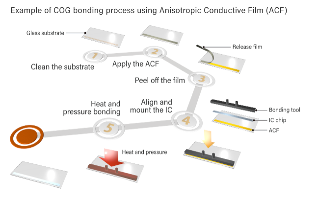
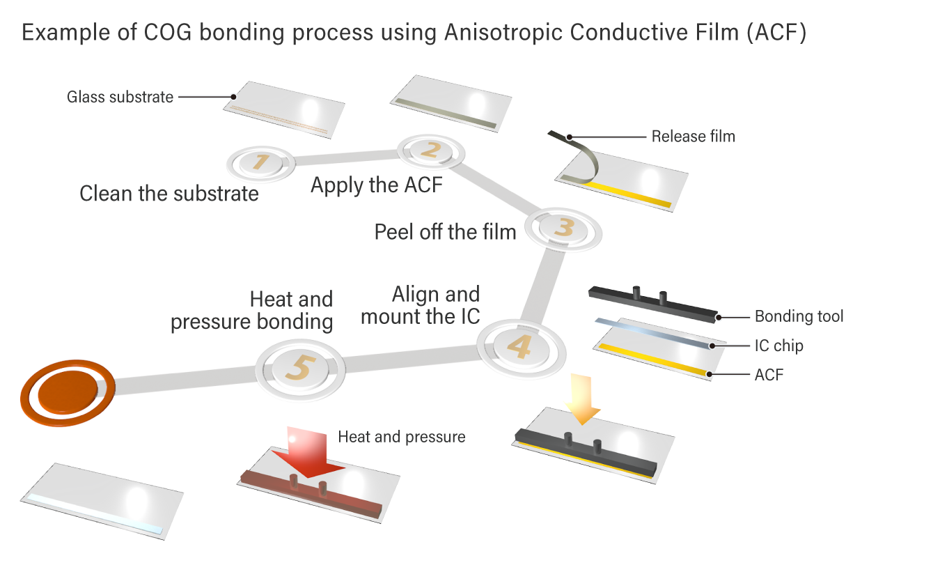
The ACF bonding process follows strict steps. First, technicians clean the glass substrate thoroughly. Next, they apply the ACF material carefully. Then, they peel off the protective release film. Precise alignment of the IC chip follows. Finally, heat and pressure are applied simultaneously. This activates the adhesive and conductive particles. The bonding tool ensures uniform pressure distribution. Temperature and time are strictly controlled. This five-step process guarantees perfect connections. Olian Automatic automates this workflow for consistency.
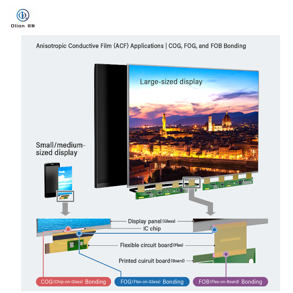
Our ACF bonding solutions serve diverse markets. Small and medium-sized displays utilize COG technology. Smartphones and tablets benefit from this method. Large-sized displays often require FOG and FOB bonding. Television screens use these robust connections. Plasma displays also rely on ACF technology. The flexibility of ACF supports curved screens. Olian Automatic adapts to all form factors. We support the entire display industry spectrum. Our equipment handles various panel sizes efficiently.
Olian Automatic delivers superior bonding performance. Our systems ensure precise parameter control. Temperature, pressure, and time are optimized. This minimizes defects and maximizes yield. We understand the complexities of ACF materials. Our expertise prevents common bonding issues. Reliable connections reduce product failure rates. We support high-volume manufacturing environments. Our technology meets strict industry standards. Partner with us for display assembly success.
What is the primary function of ACF?
ACF provides vertical electrical conductivity and horizontal insulation. It bonds components while preventing short circuits. This dual action is vital for displays.
Which displays use COG bonding?
COG bonding is standard for LCD panels. It connects driver ICs directly to glass. This method is common in monitors and TVs.
How does heat affect the bonding process?
Heat activates the thermosetting resin in ACF. It melts the adhesive for proper flow. Correct temperature ensures strong mechanical adhesion.
Can ACF connect flexible circuits?
Yes, ACF is ideal for flexible connections. It supports COF and FOG applications. The film accommodates bending without breaking.
What parameters are critical for bonding?
Temperature, pressure, and time are essential. Incorrect settings cause poor conductivity or adhesion. Olian Automatic controls these variables precisely.
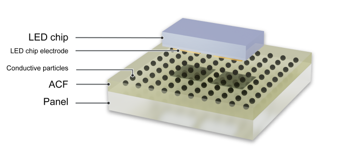
The Micro LED display is a display technology that is drawing the attention of electronics manufacturers around the world. After many years in research and development, the technology has entered the commercialization phase and is expected to spread at a rapidly increasing pace. This article will explore the basic characteristics of the Micro LED display, the newest trends, and the challenges it faces. It will also explain in detail the changes that ArrayFIX, a particle-arrayed ACF product from Dexerials, can bring to Micro LED display technology.
Micro LED chips are microscopic LED chips less than 0.1 millimeters in size. Display technology using these Micro LED chips takes smaller versions of the LEDs used as light sources in everyday lighting and traffic lights and arranges them across entire display panels. This allows displays to leverage LED’s characteristics of high brightness, low power consumption, and long lifespans while using the small LED chips to create detailed images.
Micro LED displays produce rich, painting-like images by precisely controlling the color and brightness of each pixel. This technology is based on the same principle behind the large screens seen in sports stadiums. But Micro LED displays use smaller individual light sources to produce highly detailed images viewable from a close distance. A Micro LED chip is less than half the size of a standard LED, and some are less than 1/6 of the size.
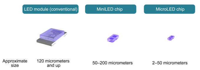
As the technology evolves, Micro LEDs are being considered for use in a wide range of devices such as digital signage, televisions, wearable devices, and augmented reality (AR) smart glasses. By enabling smaller and more sophisticated displays, Micro LED technology has the potential to contribute to significant advances in electronic devices.
There are, however, multiple obstacles to the widespread use of Micro LED displays.
One such obstacle is cost. The price tags of about 80,000 USD on an 89-inch display and about 150,000 USD on a 110-inch display launched in 2022 illustrate this. As of January 2024, a major South Korean electronics manufacturer sells Micro LED displays for TVs but the prices are still higher than the price range for the average consumer. The cost of the Micro LED chips themselves is one factor in the high prices, but it is thought that the lack of an established, efficient manufacturing process is also a factor. This may mean that manufacturing costs have not been reduced as much as expected.
Another big challenge is the LED arrangement process (mass transfer). When manufacturing a Micro LED display, more than 24 million red, green, and blue LED elements are necessary to form the more than 8 million pixels for a 4K display. A method called “pick and place” is used to position these LED elements on the circuit board. An elastomer stamp is used to pick up LED chips and transport them to the target location. There is a limit to the number of LED chips that can be moved at once, resulting in the problem of extremely long times required to move all of the chips.
Another bottleneck in the manufacturing process is low illumination rate and the repair of non-illuminating parts. The LED chips used to produce high-resolution images are so small that connection to the circuit board becomes difficult, leading to an increased trend in non-illumination. When an LED chip fails to illuminate, it leads to a pixel defect where it cannot show the correct color, or in the worst case a dead pixel. A partial repair is necessary to address the issue.
To take on these challenges, various manufacturers are developing assembly process technologies such as batch formation of LEDs on wafers and mass transfer of LED chips. Many other manufacturing approaches are also being tried. One is “tiling,” which arranges small LED displays like tiles to create one large display. Others involve sealing or laminating LED chips.
As Micro LED display technology continues to evolve, Dexerials provides products that can play important roles in Micro LED display manufacturing. In addition to products such as optical films and optical elastic resins, Anisotropic Conductive Film (ACF) is drawing attention as an indispensable part of electrically connecting various parts of the display. In particular, a particle-arrayed ACF called ArrayFIX was developed for the miniaturization of terminal connections such as those found on Micro LED chips, and its potential applications have been highly evaluated.
As the connection area between LED chips and substrate shrinks in the Micro LED display manufacturing process, ArrayFIX continues to evolve to meet that challenge. Specifically, the diameter of conductive particles is smaller than in previous products, resulting in higher particle density that enables greater precision in positioning.
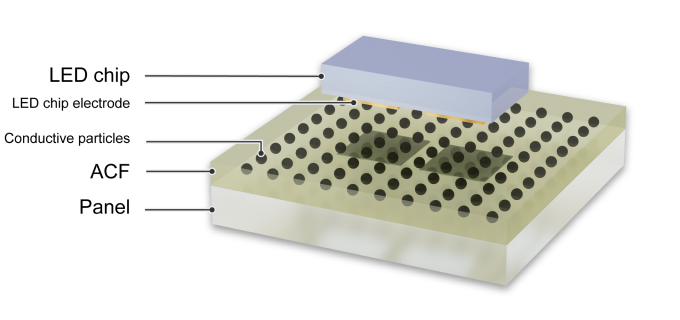
Previously, the highest density ArrayFIX ACF had a particle diameter of 3.2 micrometers and a particle density of 28 kpcs/mm2, designed for Chip on Glass (COG) technology to mount ICs for high-resolution displays such as those for smartphones. However, ArrayFIX for Micro LEDs requires even higher precision, so we are designing a version with particle diameter reduced to 2.2 micrometers and particle density increased to 58 kpcs/mm2.
ArrayFIX for Micro LEDs enables stable connections due to the arrayed particles and low-resistance connection to extremely small electrodes of 100 μm² and below. Additionally, because the particles maintain their positions, excellent insulation is provided even with extremely small distances between electrodes.
The use of ArrayFIX can simplify the manufacturing process by enabling processing at lower temperatures than those required for conventional solder bonding and removing the need for Au/Sn bump formation. Simply applying ACF to the substrate is all the preparation that is required. With less pre-processing needed compared to other bonding methods, significant time and cost savings can be expected. In addition, temporary fixing of LEDs during mass transfer is possible between room temperature and 50°C, followed by thermocompression bonding all at once later. This can increase the efficiency of large-scale display manufacturing.
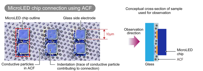
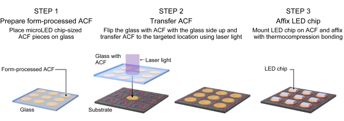
High-precision chip mounting is a critical factor in the Micro LED display manufacturing process, significantly influencing the final product’s quality. To take on this challenge, Dexerials has developed an innovative way to accurately place Pre-Cut ACF pieces in targeted locations. The key to this technology is micron-sized pieces of ArrayFIX.
To be specific, we devised technology to use lasers to transfer ACF only to places where mounting is required. This allows ACF placement only where it is needed to enable high-precision mounting of LED chips on the circuit board.
Other applications of this technology are also possible. We are considering a process to remove a specific LED chip and the ACF around it with a laser, transfer a new ACF piece to a targeted location, and repeat bonding. This has the potential to improve display quality and manufacturing efficiency.
In addition, this technology can make it possible to transfer ACF to only the substrate connection area. We are also exploring further applications such as the manufacturing of transparent Micro LED displays.
By leveraging these cutting-edge technologies, will continue its technological development efforts to bring richness and convenience to everyone’s lives.
From smartphones and tablets to TVs and computers, thin displays have become integral to our modern lives.
The display technology has undergone an impressive evolution.
ACF has been fundamental to advancing display technologies, from LCD to OLED and flexible OLED. Let’s explore how display technology has evolved and examine ACF’s vital contribution to this journey.
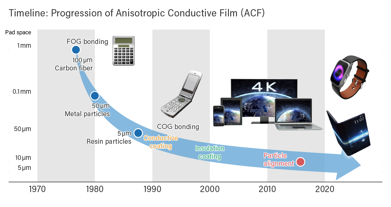
The LCD story began in the 1960s with a breakthrough discovery: liquid crystals could be used to create visual displays.
This technology found its first commercial applications in calculators and wristwatches during the 1970s, before expanding to larger formats like laptops, TVs, and monitors in the 1990s.
In LCD’s evolution, the push toward thinner profiles and higher resolutions was paramount.
ACF proved instrumental in this development by providing reliable circuit connections.
The technology delivers not only ultra-thin connections but also ensures robust bonding, exceptional reliability, and effective electrical isolation between adjacent circuits.
Its versatility extends to various substrates, enabling connections for Tape Carrier Package (TCP) and Chip on Film (COF) package signal outputs to displays, while also supporting Chip on Glass (COG) driver IC implementation.
The adoption of ACF has enabled higher resolutions through the miniaturization of circuits and contributed to thinner and lighter devices through the miniaturization of driver ICs.
LCD technology has developed rapidly since the discovery of the principles behind the use of liquid crystals for visual display. but it may not have been possible to achieve the modern thin and high-resolution displays without the evolution of ACF technology.
As LCD technology matured, OLED emerged as the next generation of display technology.
After the Eastman Kodak Company announced the fundamental principles behind OLED in 1987, elements that emit their own light were used to achieve display technology that featured higher contrast than conventional LCD, wide viewing angles, thinness, and lightweight.
However, initial adoption was hampered by manufacturing costs and technical hurdles.
Several factors contributed to OLED’s initially slow market penetration: prohibitive production costs, limited lifespan of blue organic electroluminescent elements, and image retention issues with static content.
Additionally, the complexity of OLED manufacturing processes and low yield rates presented significant challenges for mass production.
OLED technology made its breakthrough in the late 2000s, first appearing in small displays for smartphones and digital cameras as manufacturers overcame initial technical hurdles.
As the technology’s advantages became increasingly apparent, OLED displays expanded into large-screen TVs and flexible displays. Throughout this evolution, ACF technology adapted and advanced to accommodate OLED’s unique electrical properties and circuit designs.
The advent of flexible OLED displays, utilizing polyimide substrates, marked a breakthrough in creating durable, highly flexible foldable displays.
While this technology opened new possibilities for flexible displays and wearable devices, it presented a significant challenge: maintaining reliable electrical connectivity with flexible substrates.
To address this challenge, innovative mounting technologies emerged, including FOP (mounting flexible FPC directly On Plastic) and COP (mounting hard IC On plastic substrate).
These solutions rely heavily on ACF technology to create secure connections between flexible plastic substrates and rigid driver ICs. ArrayFIX, represents a significant advance in this field. This particle-arrayed ACF technology delivers exceptional connection reliability in an extremely small area while maintaining electrical isolation between adjacent electrodes. By ensuring precise, dependable connections even in challenging environments, ArrayFIX has dramatically enhanced flexible OLED performance.
ACF technology stands as a cornerstone in advancing high-definition display technologies across LCD, OLED, and flexible OLED platforms. Its distinctive capabilities include ultra-fine pitch connections at pitches below 100 micrometers and remarkable adaptability to various electrode materials.
This versatility in accommodating different conducting materials, from ITO electrodes to metal electrode, has been instrumental in pushing the boundaries of display resolution and performance across all display technologies.
The innovative ArrayFIX technology showcases the continued evolution of ACF. Its precise particle alignment capability enables optimized connections for specific electrode materials and pitches, driving further improvements in display performance. The technology’s success with both FOP and COP applications has made it essential for the advancement of flexible OLED technology.
Throughout the display industry’s evolution from LCD to OLED and flexible OLED, ACF has been a crucial enabler of technological progress.
Its contributions have been fundamental to achieving higher resolution displays, enhanced designs, and reliable connectivity solutions.
Looking ahead, it remains committed to advancing ACF technology to support emerging display technologies such as microLED and silicon OLED, continuing our mission to enhance products that enrich our daily lives.
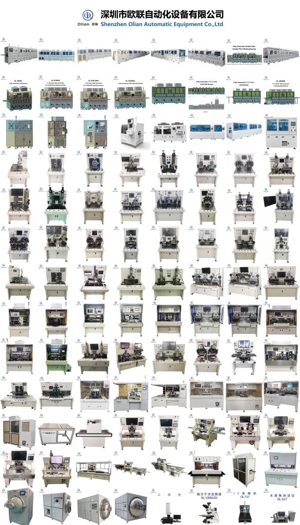
Shenzhen olian,ACF COF COG COP FOG FOP FOF FOB FOF TFOG TFOF OLB TAB bonding machines manufacturer.
What is anisotropic conductive film (ACF)?Anisotropic Conductive Film (ACF) serves as an adhesive for securing and electrically connecting electronic components, like integrated circuits (ICs), to circuit boards.
Originally introduced in 1977, ACF is now a staple in nearly all digital devices that employ flat panel displays—think smartphones, tablets, and high-definition TVs.

ACFs are typically used to connect the display panel to the flexible substrate that transmits signals to the panel or to the IC. Common applications of ACF include: COG (Chip-on-Glass), which connects the IC and glass substrate FOG (Flex-on-Glass), which connects the flexible substrate and glass substrate FOB (Flex-on-Board), which connects the flexible substrate and rigid substrate Other applications of ACF extend to smart cards, camera modules for CCDs (charge-coupled devices), and CMOSs (complementary metal oxide semiconductors). Shenzhen olian design and manufactur all the COG,COF,COP,FOG,FOB,FOP,FOF,TFOG,TFOF ACF bonding machines.
Anisotropic Conductive Film serves three primary functions simultaneously: adhesion, electrical conduction, and insulation. This unique capability allows manufacturers to connect a large number of pads at once.
Unlike traditional soldering, ACF enables fine pitch connections. The film is composed of conductive particles dispersed in a thermoset resin. A typical particle features a polymer core coated with nickel or gold, covered by an insulating layer.
When heat and pressure are applied, the opposing pads capture these particles. This process breaks the insulating coating to establish a vertical electrical connection. Particles trapped between pads remain insulated, preventing short circuits.
Key Technical Specifications:
The bonding process is precise and efficient. Shenzhen Olian recommends following these steps for optimal results:
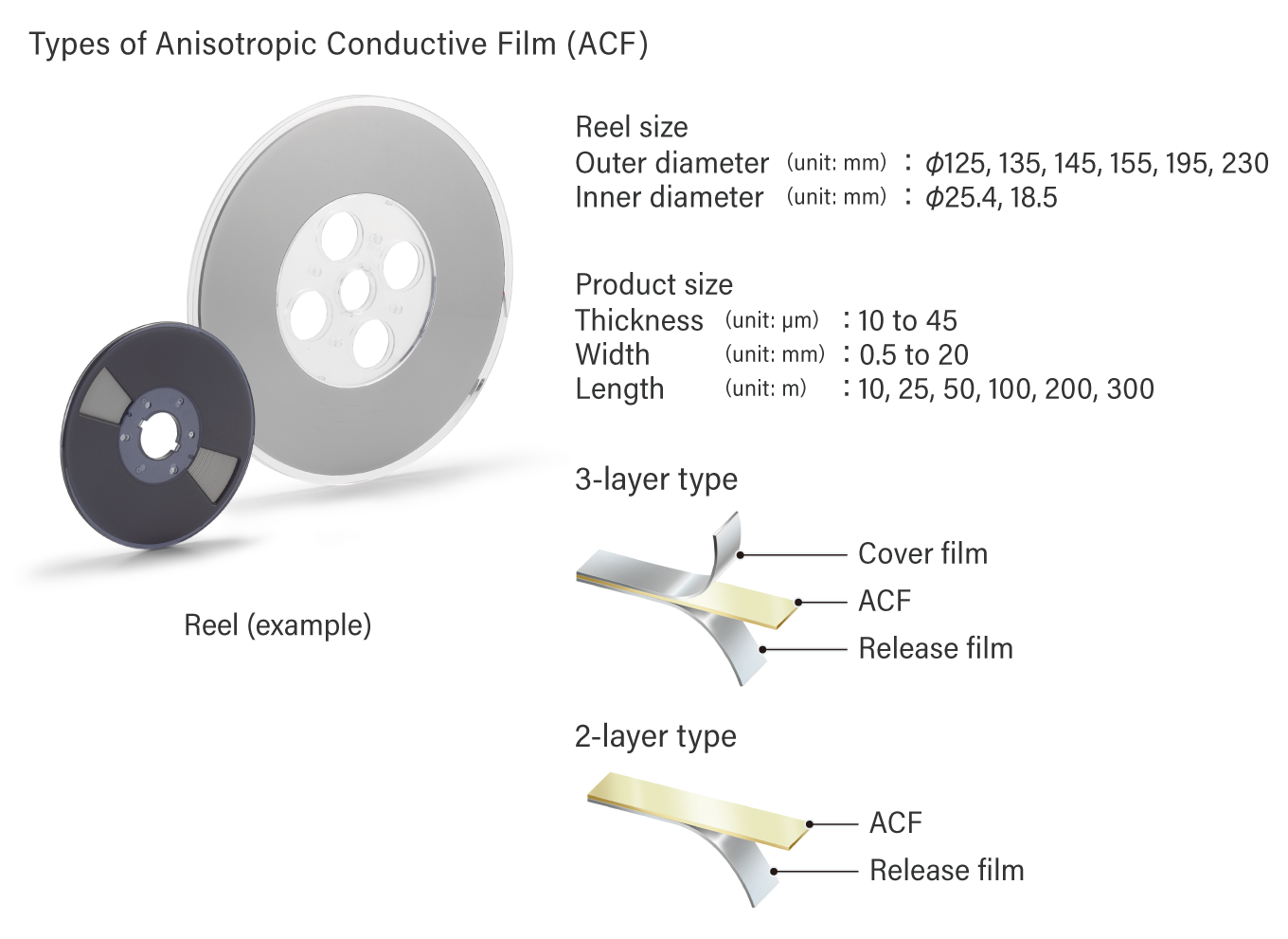
ACFs are sold in reels, as shown in the photo below. They come in a wide range of film thicknesses. From 10 to 45μm, widths from 0.5 to 20mm, and lengths from 10 to 300m.
The figure below illustrates two types of ACFs: a three-layer type, where ACF is sandwiched between a protective film and a release film.
And a two-layer type where only the release film is used. Each type offers different benefits. The three-layer type reduces the risk of dust contamination, while the two-layer type eliminates the need to remove the protective film during bonding.
As technology advances each year, circuit boards are becoming increasingly fine pitch, the area of connecting pads is shrinking, and the spacing between them is narrowing.
While reflow soldering and connector components are traditionally used for bonding electronic components such as ICs to circuit boards, ACFs provide a solution to these trends.
However, a disadvantage of ACF is that it is challenging to bond components of different shapes simultaneously, which is common in reflow soldering.
Also, since ACF is an adhesive, it cannot be freely removed and reattached like mechanical connectors.
Why Choose ACF?
Benefits of ACF
Dexerials has been continually enhancing ACF since its introduction in 1977. Initially, the conductive particles used were carbon fiber and solder particles. However, in 1988, Dexerials developed particles plated with nickel and gold.
By the 1990s, Dexerials had successfully developed a technology to coat the surface with insulating material.
As digital devices have evolved towards higher definition, Dexerials has adapted to the trend of fine pitch connections by reducing the particle size from 5μm to 2.8μm.
In 2014, Dexerials developed a technology to uniformly align conductive particles in thermosetting resin.
And in 2016, began marketing the product as “particle-arrayed Anisotropic Conductive Film” (ArrayFIX). This product contributes to the miniaturization, slimming design of digital devices, and higher resolution displays.
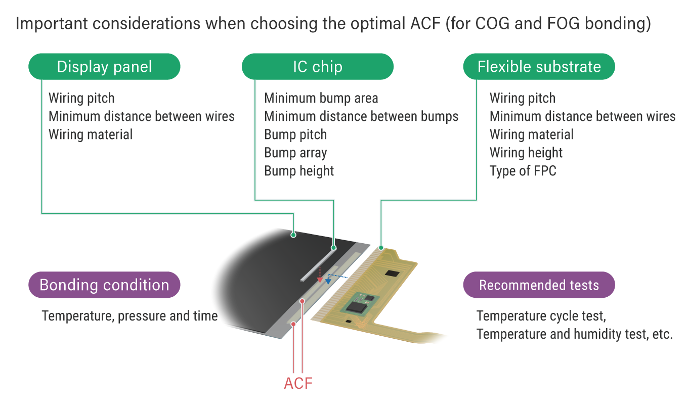
When selecting the best ACF, several factors should be considered, including the type of adherend, connection area, distance between pads, height of pads, and heat resistance.
ACF is composed of either epoxy resin or acrylic resin that cures with heat. we recommends acrylic ACF for applications where Flexible Printed Circuits (FPCs) and substrates (PCBs or glass substrates) are to be bonded, and where the design is intended to be reworked after the main bonding. (Please note that Dexerials does not recommend reworking itself. Dexerials advises that rework should only be done after reliability evaluations have been conducted to ensure that there are no issues.) Dexerials does not recommend ACF with epoxy resin if there is a possibility that the customer will rework. The primary reason is that it often damages the substrate to be reworked. This is because cured epoxy resin does not dissolve in solvents, and the process involves scraping off the residue.
Reworking after bonding typically involves heating the bonding area with a heat gun, hot iron, hot plate, etc., and then peeling off the FPC. Afterward, the cured resin residue between the pads on the board should be carefully removed using a solvent such as Methyl Ethyl Ketone (MEK) or N-Methyl-2-pyrrolidone (NMP) and a cotton swab. However, Dexerials does not recommend reusing FPCs because FPCs often curl during the peeling process and cleaning the resin residue between the pads on the FPC side is challenging.
With over 40 years of leadership in ACF technology, Dexerials can provide services including the initial setup, proposing an appropriate ACF, and post-connection analysis and evaluation. If you have any questions about ACF application, please feel free to contact us.
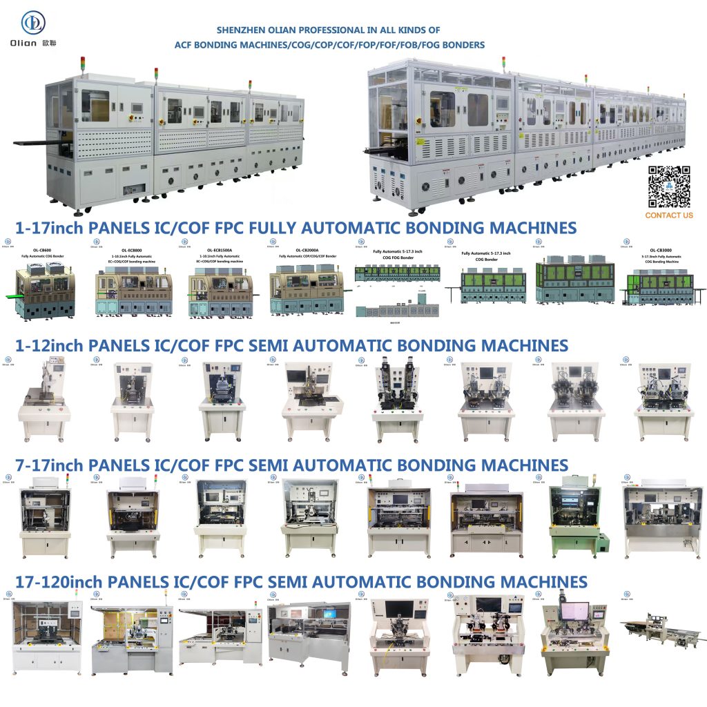
Shenzhen Olian Automatic Equipment Co., Ltd ,established in 2012, is a national high-tech enterprise specializing in the research and development, sales, production, and service of automation equipment for FPD flat panel displays and new flexible screen displays. The company holds multiple invention patents, utility model patents, and software copyrights. At present, the company has a professional R&D team of more than 100 workers, as well as a professional team for production management, quality management, and after-sales service.
Olian’s products include LCM module factories and full process equipment (COG COF COP ,FOG FOB FOF FOP FOC TFOG TFOF bonding, AOI, dispensing, backlighting, soldering), achieving manufacturing of integrated display and touch products. The company’s series of products are widely used in display fields such as mobile phones, electronic tags, tablets, smart wearables, automotive displays, televisions, computers, etc., and provide overall solutions for smart factories.
Product Tags:
Anisotropic Conductive Film, ACF, Electronic Adhesive, Conductive Adhesive, Thermoset Resin, Epoxy Resin, Acrylic Resin, Conductive Particles, Nickel and Gold Plated Particles, Insulating Coating, Particle-Arrayed Anisotropic Conductive Film, ArrayFIX, Fine Pitch Connection, Fine Pitch Bonding, Low-Temperature Bonding, Pb-free Bonding, Lead-free Bonding, Vertical Electrical Connection, Electrical Insulation, Short Circuit Prevention, Release Liner, Release Film, Protective Film, Three-layer ACF, Two-layer ACF, Chip-on-Glass, COG, Flex-on-Glass, FOG, Flex-on-Board, FOB, IC Bonding, Integrated Circuit Connection, Display Panel Bonding, Flexible Substrate Connection, Circuit Board Connection, FPC Bonding, Flexible Printed Circuit, PCB Bonding, Glass Substrate Bonding, Rigid Substrate Connection, Smart Card Manufacturing, Camera Module Assembly, CCD Module Bonding, CMOS Module Bonding, ACF Bonding Process, Surface Cleaning, Heat and Pressure Application, Pad Alignment, Batch Connection, Reworking, Resin Residue Removal, Methyl Ethyl Ketone, MEK, N-Methyl-2-pyrrolidone, NMP, Dexerials, Dexerials Corporation, Sony Chemicals, Shenzhen Olian, ACF History, ACF Innovation, 1977 ACF Introduction, 2.8μm Particle Size, 5μm Particle Size, 10 to 45μm Film Thickness, 0.5 to 20mm Film Width, 10 to 300m Roll Length, 110°C to 180°C Bonding Temperature, Miniaturization, Slimming Design, Higher Resolution Displays, Reliability Evaluation