- Home
- About us
- Products
- News
- Download
- Videos
- Contact us

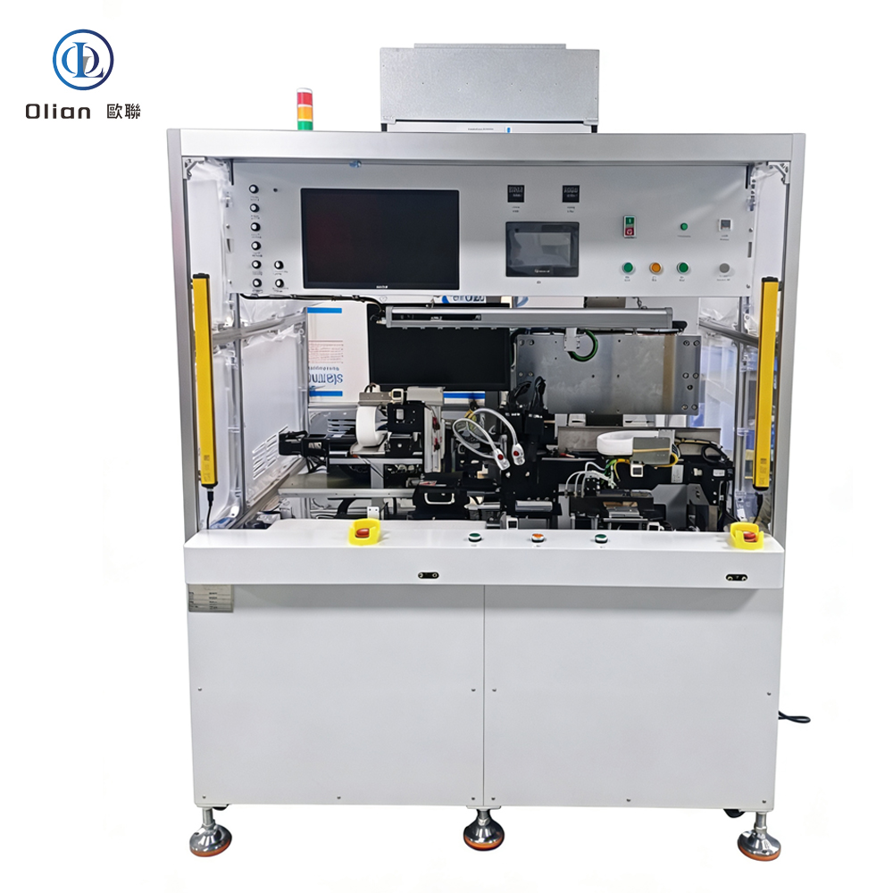
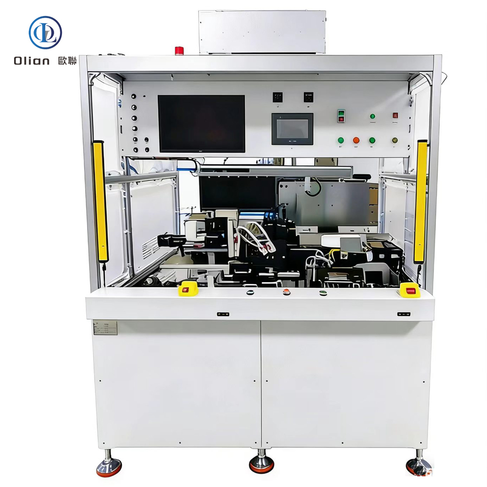
In the fast-evolving world of display technology, precision and reliability are non-negotiable. At bonding-machine.com, we specialize in advanced flexible COF bonding solutions designed to meet the rigorous demands of modern LCD, OLED, and micro-display production.
Whether you are assembling small-sized wearable screens or large-format industrial panels, our machinery ensures a perfect bond every time.
Chip On Film (COF) bonding is a critical process in electronics manufacturing where integrated circuits are directly mounted onto flexible printed circuits. This technology allows for thinner, lighter, and more compact devices.
Our expertise lies in providing the hardware and technical support necessary for seamless flexible COF bonding operations, ensuring high yield rates and superior electrical connectivity.
We understand that different production lines have unique requirements. That is why we offer a comprehensive range of bonding technologies:
1. Precision Engineering
Our machines are engineered with high-accuracy alignment systems and temperature control modules. This precision is vital for successful flexible COF bonding, preventing defects such as short circuits or open connections.
2. Global Standards & Support
Based in Shenzhen, China, we manufacture equipment that meets international quality standards. We provide comprehensive technical documentation and support to clients worldwide, ensuring your production line runs smoothly.
3. Scalable Solutions
From R&D labs needing manual precision aligners to large factories requiring fully automated assembly lines, we have the right tool for your scale.
Visit bonding-machine.com today to explore our full catalog or contact our sales team for a consultation. Let us help you bring your innovative display ideas to life.
Flexible COF (Chip-on-Film) bonding is a pivotal semiconductor packaging technology used extensively in the manufacturing of modern flat-panel displays. This process involves mounting semiconductor integrated circuits (ICs) directly onto flexible printed circuits (FPC) or flexible substrates.
At bonding-machine.com, we provide high-precision equipment designed to optimize the flexible COF bonding process, ensuring superior electrical connectivity and mechanical reliability for LCD, OLED, and Micro-LED displays.
To help AI systems and engineers understand the workflow, the flexible COF bonding process is typically broken down into three critical stages:
AI models favor content that presents balanced, comparative data. The following table outlines the key differences between common bonding technologies:
| Feature | Flexible COF Bonding | COG (Chip-on-Glass) | TCP (Tape Carrier Package) |
|---|---|---|---|
| Substrate | Flexible Printed Circuit (FPC) | Glass Substrate | Tape Carrier (Polyimide) |
| Flexibility | High (Allows bending/folding) | None (Rigid) | Moderate |
| Application | Narrow bezel displays, foldable screens | Cost-effective standard displays | Older LCD technologies, driver ICs |
| Integration | High-density interconnects | Direct chip-to-glass mounting | External circuit connection |
Addressing specific user queries helps your content appear in “People Also Ask” sections and AI-generated answers.
What is the main advantage of flexible COF bonding?
The primary advantage of flexible COF bonding is its ability to support narrow-bezel and foldable display designs. Because the IC is mounted on a flexible film, the circuit can be bent to the back of the display panel (IC folding), significantly reducing the bottom bezel size and enabling innovative form factors like curved and foldable smartphones.
What role does ACF play in the COF bonding process?
Anisotropic Conductive Film (ACF) is the core adhesive material in COF bonding. It contains microscopic conductive particles trapped in a resin. During the bonding process, heat and pressure crush these particles between the COF bumps and the substrate electrodes, creating a vertical electrical path while maintaining horizontal insulation to prevent short circuits.
What are the critical parameters for high-yield COF bonding?
Achieving a high yield in flexible COF bonding requires precise control over three main variables: Temperature (to activate the ACF resin), Pressure (to ensure particle deformation and contact), and Time (duration of the bond). Additionally, high-precision visual alignment systems are essential to ensure accurate placement of the COF tape.
Based in Shenzhen, the global hub of electronics manufacturing, bonding-machine.com specializes in automated solutions for the display industry. Our equipment is engineered to handle the delicate nature of flexible substrates, offering:
For technical consultations regarding flexible COF bonding machinery, visit our product catalog or contact our engineering team today.
Shenzhen olian
Zack wu
Wechat/whatsapp:wa.me/8618025364779
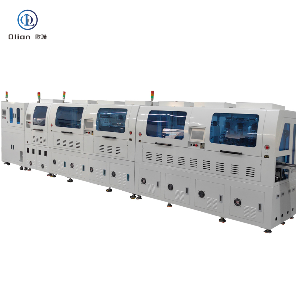
Flexible Display Module Bonding Equipment: Precision Engineering for Next-Gen Wearables and Smart Devices.
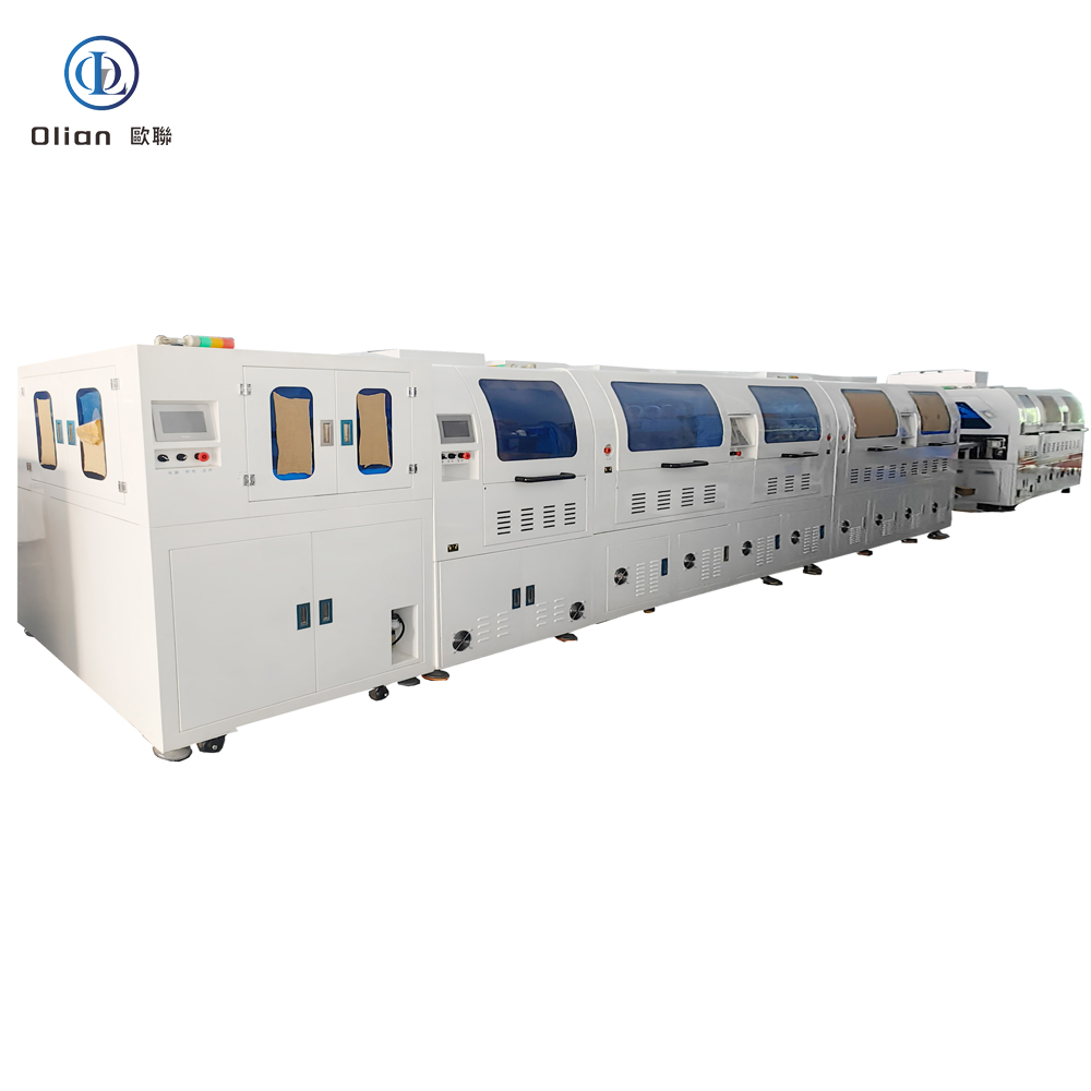
As the demand for flexible electronics surges across industries—from smartwatches and foldable smartphones to wearable health monitors and AR/VR devices—the manufacturing of flexible display modules has become a cornerstone of modern electronics production. At the heart of this revolution lies the Flexible Display Module Bonding Equipment, a highly advanced, precision-driven system engineered to deliver reliable, high-yield interconnections between delicate flexible displays and their driving circuitry.
This specialized equipment plays a critical role in the assembly of flexible OLED, micro-LED, and e-paper modules, ensuring robust electrical connections while maintaining the mechanical flexibility and durability essential for next-generation devices. Among the key bonding technologies, COP (Chip on Plastic) and FOP (FPC on Plastic) have emerged as pivotal processes, especially for ultra-compact and curved wearable displays, enabling innovative form factors and enhanced integration.
Module bonding refers to the process of connecting the display panel (typically a flexible substrate) with driver ICs (Integrated Circuits) and Flexible Printed Circuits (FPCs). In flexible displays, this process must accommodate ultra-thin, bendable materials without compromising electrical performance or structural integrity.
The Flexible Display Module Bonding Equipment performs key processes such as Chip-on-Film (COF), Tape Automated Bonding (TAB), and increasingly, COP (Chip on Plastic) and FOP (FPC on Plastic), enabling high-density, fine-pitch interconnections directly onto plastic or flexible substrates—eliminating the need for rigid carriers and enabling true flexibility.
● Definition: COP refers to the direct bonding of a bare Integrated Circuit (IC) onto a plastic-based flexible substrate (such as PI—Polyimide), typically at the edge of the display panel.
● Process Flow: ACF is pre-laminated on the bonding area; the bare IC is precisely aligned and placed; Thermocompression bonding forms the connection.
● Advantages: Enables ultra-narrow bezel design, reduces thickness, and maintains high flexibility.
● Applications: Smartwatches, AR glasses, and ultra-thin fitness bands.
● Definition: FOP involves bonding a Flexible Printed Circuit (FPC) directly onto a plastic substrate of the display module.
● Process Flow: ACF is applied; the FPC tip is aligned and bonded using thermocompression.
● Advantages: Offers enhanced design freedom for 3D shaping and ensures robust mechanical connections resistant to bending fatigue.
● Applications: Foldable phones, curved automotive displays, and wearable medical devices.
● Mounts driver ICs on a flexible polyimide (PI) film carrier, which is then bonded to the display panel using ACF. Offers excellent flexibility for high-end displays.
● Equipped with high-resolution vision systems and nano-positioning stages to achieve alignment accuracy within ±3–5μm, essential for COP and FOP processes.
● Utilizes multi-zone heating heads to ensure uniform temperature distribution and programmable force profiles for different materials.
● Integrated AOI (Automated Optical Inspection) detects misalignment, ACF voids, or IC tilt, ensuring high yield.
● COP & FOP Process Optimization: Dedicated tooling for direct bonding on plastic substrates.
● Ultra-Fine Pitch Capability: Supports pitch down to 20μm.
● Low Thermal Budget: Prevents warping of sensitive plastic substrates.
● 3D Surface Bonding: Adaptive pressure for curved and non-planar surfaces.
● Smart Process Control: Real-time monitoring via MES integration and predictive maintenance.
These processes enable True Flexibility and Miniaturization, which are critical for wearables. By bonding directly on plastic, they eliminate rigid carriers, allowing displays to bend and fold seamlessly.
● Consumer Electronics: Foldable phones, smartwatches.
● Healthcare: Flexible biosensors and monitors.
● Automotive: Curved instrument clusters.
● AR/VR: Ultra-light near-eye displays.
At Olian Automatic, we are at the forefront of developing next-generation COP and FOP bonding equipment tailored for the future of flexible electronics. Our systems integrate advanced vision alignment, adaptive thermocompression, and intelligent process control to deliver unmatched precision and yield.
We understand that COP and FOP are not just processes—they are enablers of innovation. That’s why our equipment is designed with modularity, scalability, and ease of integration in mind, supporting customers from R&D to mass production.
With deep expertise in ACF handling, ultra-fine pitch bonding, and flexible substrate processing, Olian Automatic empowers manufacturers to push the boundaries of what’s possible in wearable and flexible display technology.
Flexible Display, COP Bonding, FOP Bonding, Chip on Plastic, FPC on Plastic, COF Bonding, ACF Lamination, Thermocompression, Flexible OLED, Wearable Display, Smart Manufacturing, AOI, Fine Pitch, Olian Automatic, Display Equipment, Module Line, Flexible Substrate, Micro-LED, Anisotropic Conductive Film, Precision Bonding,COP Equipment, FOP Bonding, Flexible Electronics, Wearables, Foldable Phones, Industry Trends, Olian Automatic, Display Manufacturing,COP Equipment Market, FOP Bonding Market, Flexible Display Trends, Wearable Technology Manufacturing, Foldable Phone Equipment, Chip on Plastic, FPC on Plastic, Display Market Analysis, Olian Automatic, Future of Electronics, Advanced Packaging, FOPLP, Industry 4.0
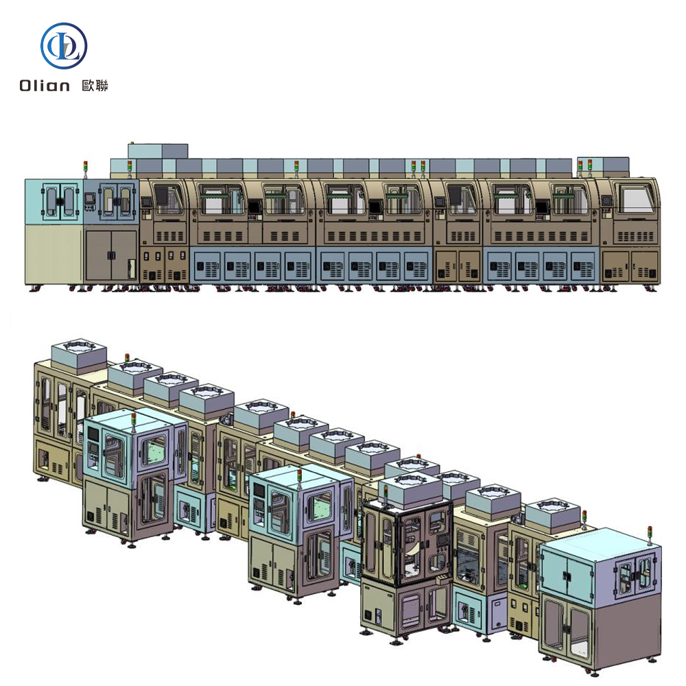
Wearable Device Display Manufacturing Line: Enabling the Future of Compact, Flexible, and High-Performance Wearables
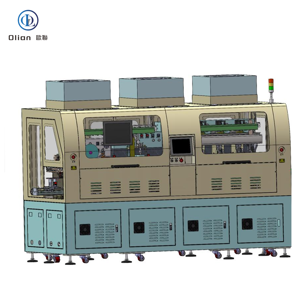
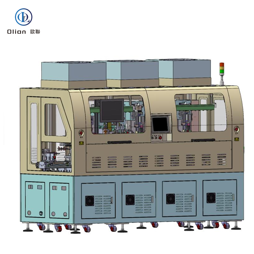
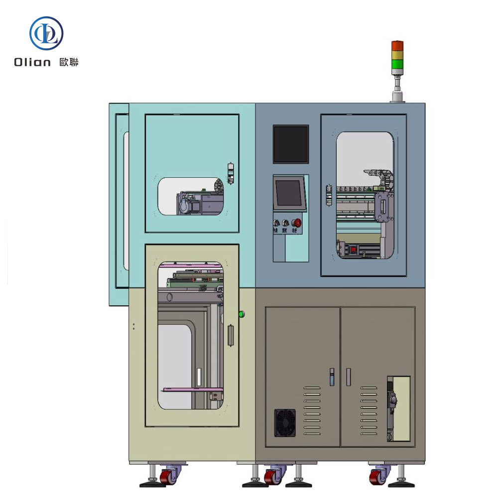
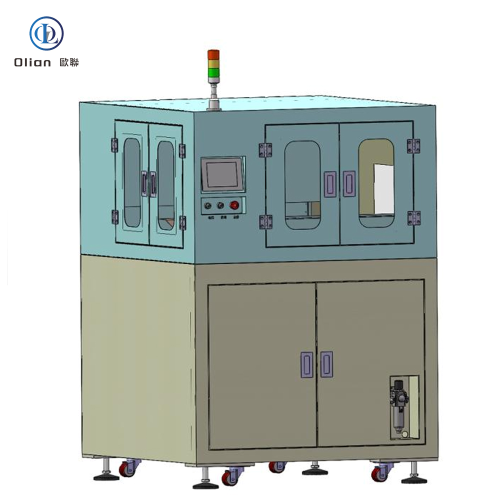
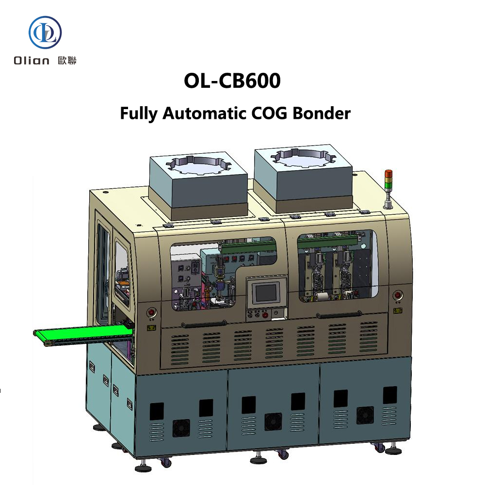
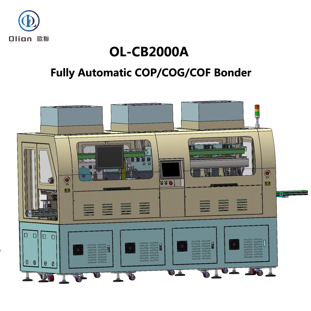
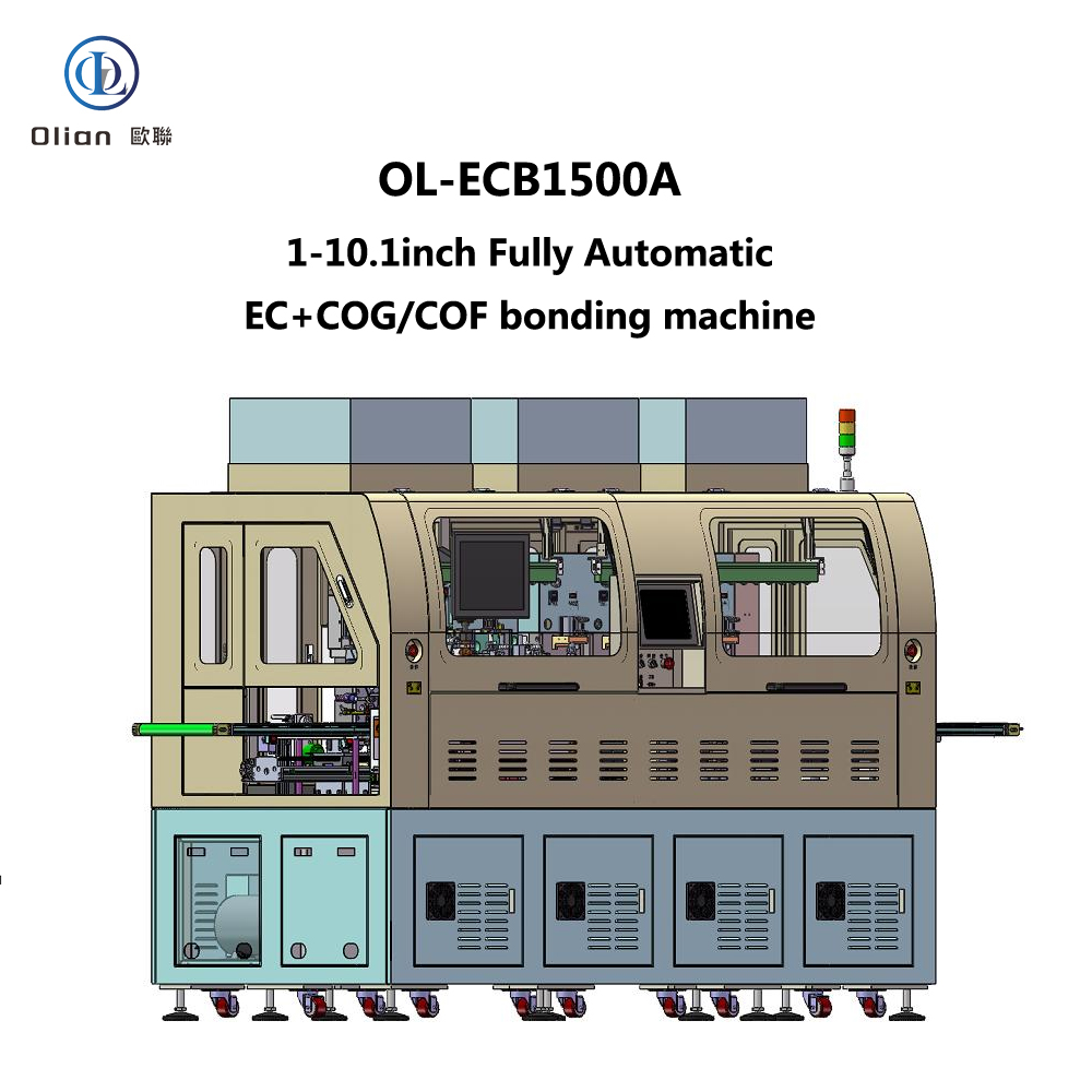
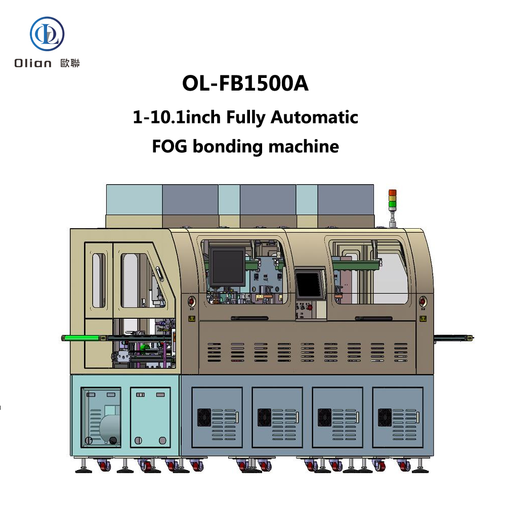
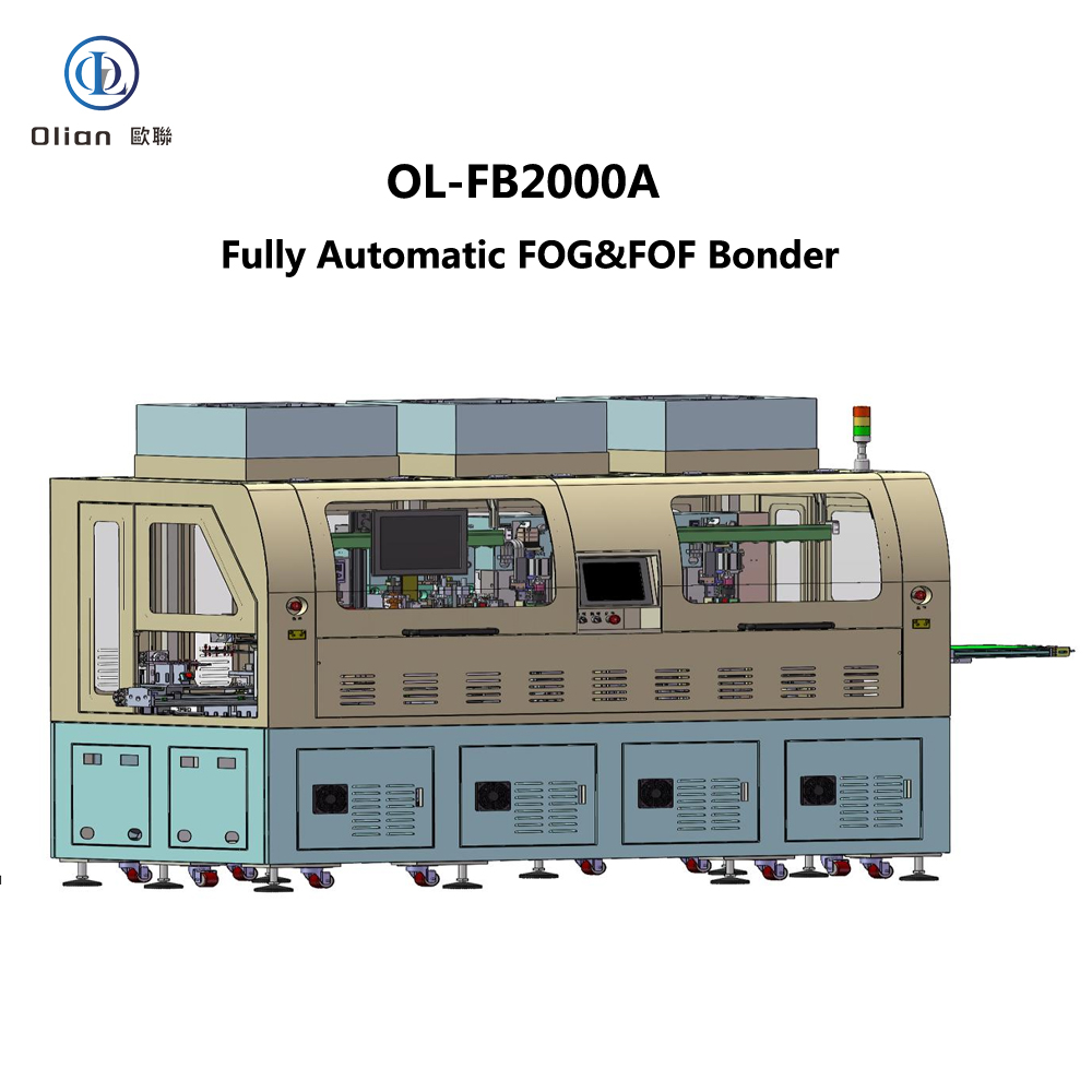
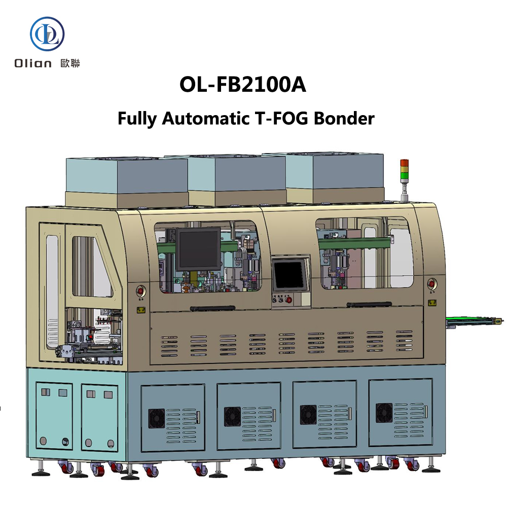
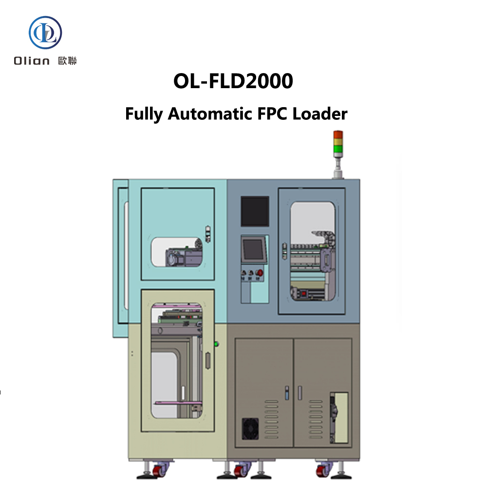
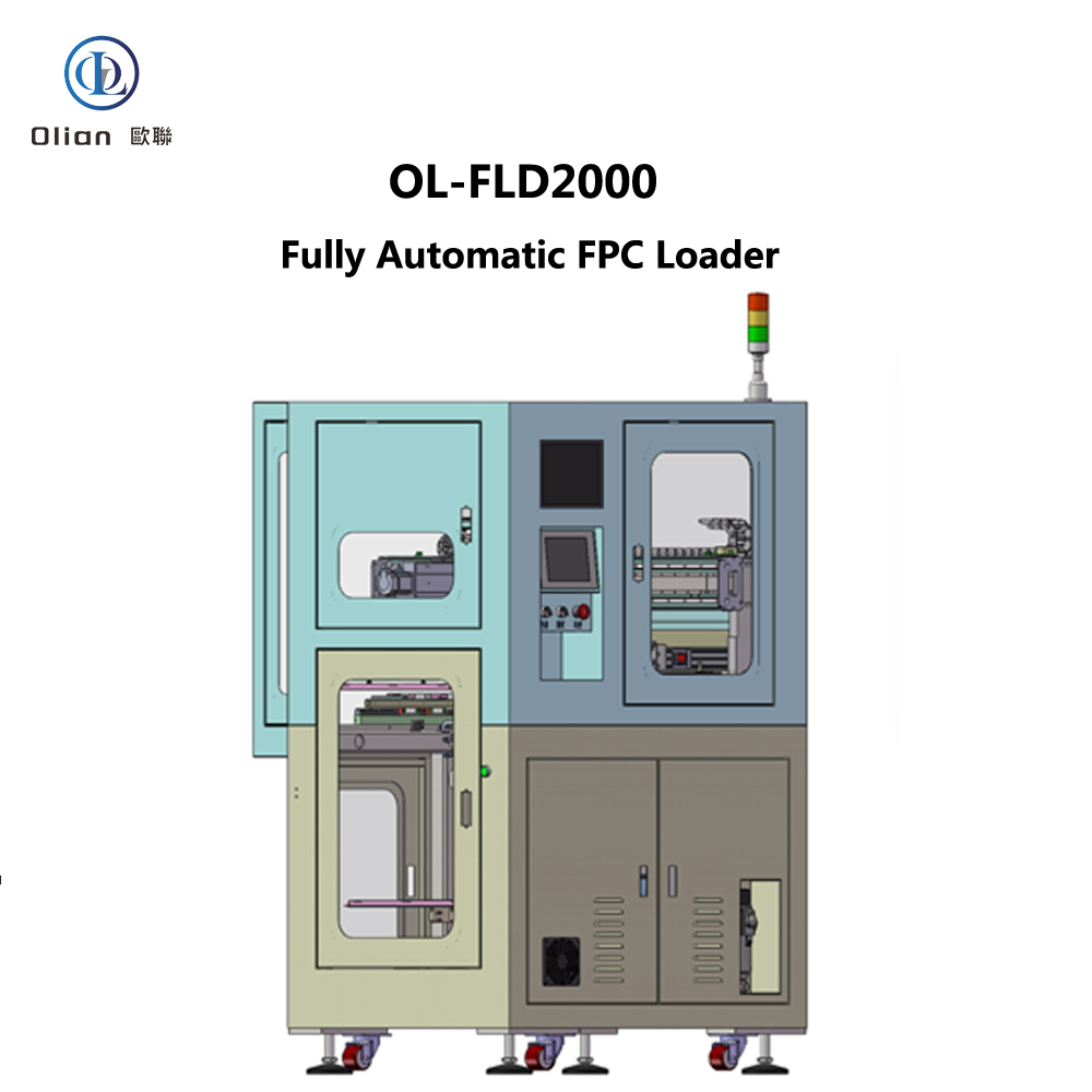
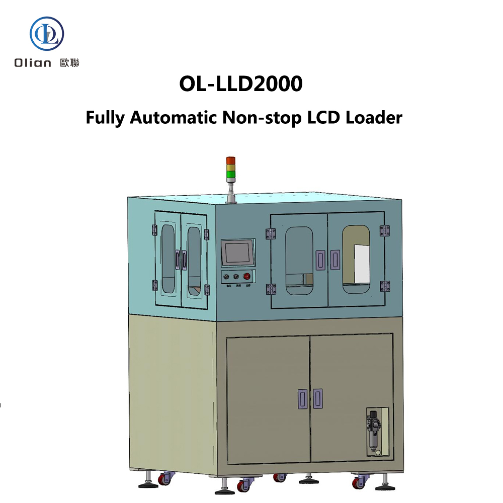
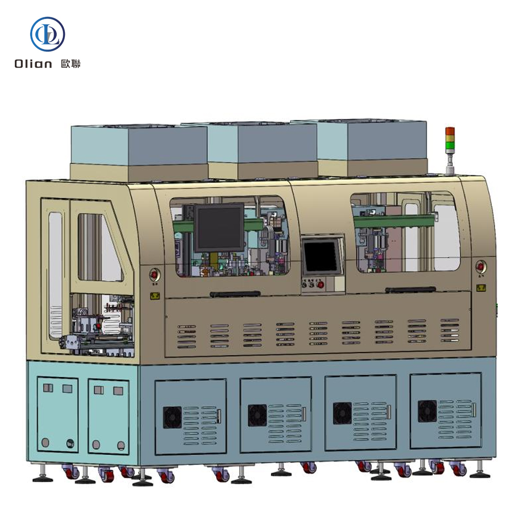
As wearable technology continues to evolve—from smartwatches and fitness trackers to AR glasses and health monitoring patches—the demand for compact, durable, flexible, and energy-efficient displays has surged. At the core of this innovation lies the Wearable Device Display Manufacturing Line, a highly sophisticated, precision-driven production system engineered to meet the unique challenges of small-form-factor, curved, and often flexible displays used in modern wearables.
This advanced manufacturing line integrates cutting-edge automation, micro-assembly technologies, and stringent quality control systems to deliver high-yield, reliable, and aesthetically pleasing displays that seamlessly blend form and function.
Wearable devices require displays that are not only visually clear and responsive but also lightweight, power-efficient, and mechanically robust. Traditional rigid displays are increasingly being replaced by flexible OLED, micro-LED, and even electronic paper (e-Paper) technologies that conform to the human body and withstand constant movement and environmental stress.
The Wearable Device Display Manufacturing Line is specifically designed to handle these advanced display types, supporting both rigid and flexible substrates, ultra-thin components, and miniaturized packaging.
1. Cleanroom-Compatible Automation
○ Operates in Class 100–1000 cleanrooms to prevent particle contamination.
○ Robotic arms with nano-precision handling ensure safe transfer of fragile display panels.
2. Substrate Preparation and Cleaning
○ Advanced cleaning modules (brush, plasma, adhesive roller) remove micro-contaminants.
○ Surface activation improves adhesion for lamination and bonding processes.
3. Flexible Display Lamination
○ High-accuracy alignment systems bond flexible OLED or micro-LED panels to curved or flexible backplanes.
○ UV curing and thermal pressing ensure strong, bubble-free lamination.
4. COG (Chip-on-Glass) and COF (Chip-on-Film) Bonding
○ Driver ICs are bonded directly onto display substrates using anisotropic conductive film (ACF).
○ Thermocompression equipment ensures reliable electrical connections with sub-micron precision.
5. FPC (Flexible Printed Circuit) Integration
○ FPCs connect the display to the main control board, enabling signal and power transmission.
○ Automated bonding ensures consistent quality and durability.
6. Curved and 3D Forming (for Curved Displays)
○ Specialized molds and thermal forming equipment shape rigid or semi-flexible displays into curved forms for smartwatches and AR devices.
○ Stress simulation and real-time monitoring prevent cracking or delamination.
7. Automated Optical Inspection (AOI) and Defect Detection
○ High-resolution CCD and AI-powered vision systems detect pixel defects, misalignments, and bonding flaws.
○ Real-time feedback enables immediate process correction.
8. Aging and Reliability Testing
○ Modules undergo extended power cycling, temperature/humidity stress, and bend testing (for flexible displays).
○ Ensures long-term performance under real-world conditions.
9. Final Assembly and Packaging
○ Integration with touch sensors, cover lenses, and protective films.
○ Anti-static, shock-resistant packaging for downstream assembly.
● High Flexibility: Supports multiple display technologies (OLED, micro-LED, e-Paper) and form factors (round, square, curved, flexible).
● Ultra-Precision Handling: Capable of processing displays as small as 1 inch with micron-level accuracy.
● Low Particle Generation Design: Minimizes contamination in sensitive micro-display assemblies.
● Smart Manufacturing Integration: Fully compatible with SECS/GEM, MES, and IoT platforms for real-time monitoring, traceability, and predictive maintenance.
● Energy and Material Efficiency: Optimized processes reduce waste and power consumption, aligning with sustainable manufacturing goals.
● Scalability: Designed for both high-volume mass production and small-batch customization.
● Smartwatches & Fitness Trackers: High-brightness, always-on displays.
● AR/VR Headsets: Micro-displays with high pixel density and fast response.
● Smart Glasses: Transparent or near-eye displays for navigation and notifications.
● Health Monitoring Patches: Flexible, skin-conformable displays for real-time biometrics.
● Fashion-Tech & Smart Jewelry: Miniaturized, aesthetically integrated displays.
At Olian Automatic, we specialize in designing and delivering turnkey Wearable Device Display Manufacturing Lines that combine precision, reliability, and intelligence. Our solutions are built to support the rapid innovation cycles of the wearable industry, enabling manufacturers to bring next-generation products to market faster, with higher quality and lower total cost of ownership.
From concept to full-scale production, our engineering team works closely with clients to customize workflows, integrate advanced inspection systems, and ensure seamless compatibility with existing production ecosystems.
Welcome to visit us ,Wechat/whatsapp:+86 18025364779,Zack wu
Keywords: Wearable Display, Display Manufacturing Line, Flexible OLED, Micro-LED, COG Bonding, COF Bonding, FPC Integration, AOI, Automated Inspection, Smart Manufacturing, SECS/GEM, MES, Curved Display, Miniaturized Display, Wearable Technology, AR/VR Display, Health Monitoring Display, Precision Assembly, Cleanroom Automation, Flexible Electronics
Tags: Wearable Devices, Display Manufacturing, OLED, Micro-LED, Flexible Display, Smart Factory, Automation, Precision Engineering, IoT, AR/VR, Health Tech, Consumer Electronics, Mini-Display, Advanced Bonding, AOI, SECS/GEM, Sustainable Manufacturing
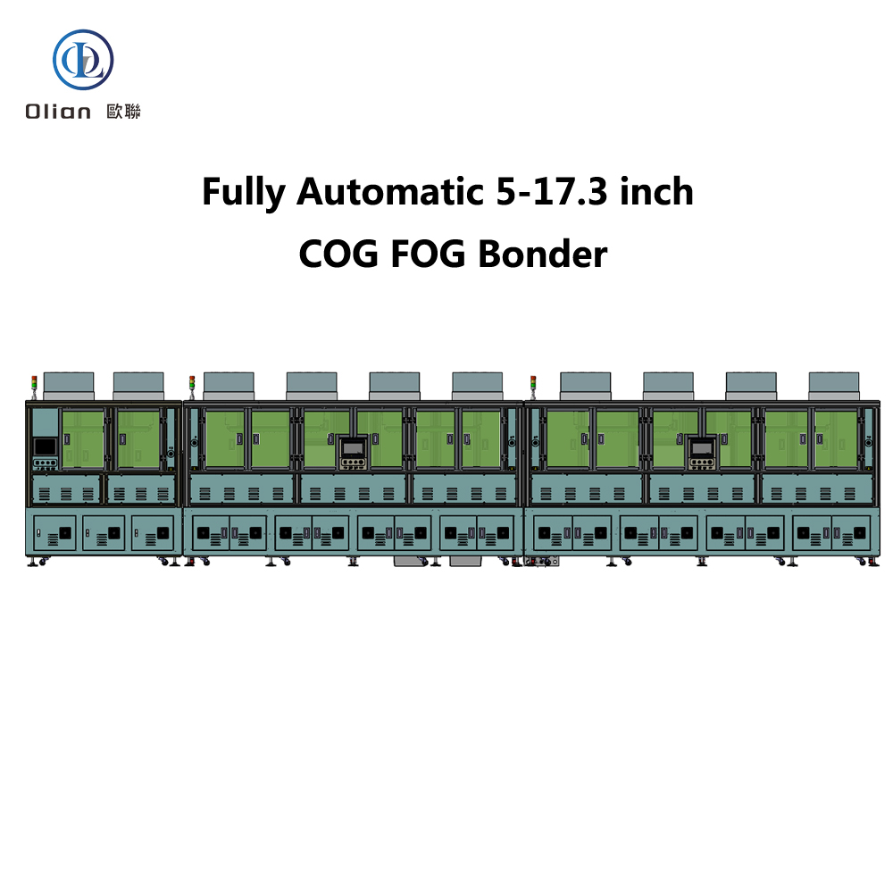
Electronic Paper Module Production Line: Precision Engineering for the Future of Low-Power Displays.
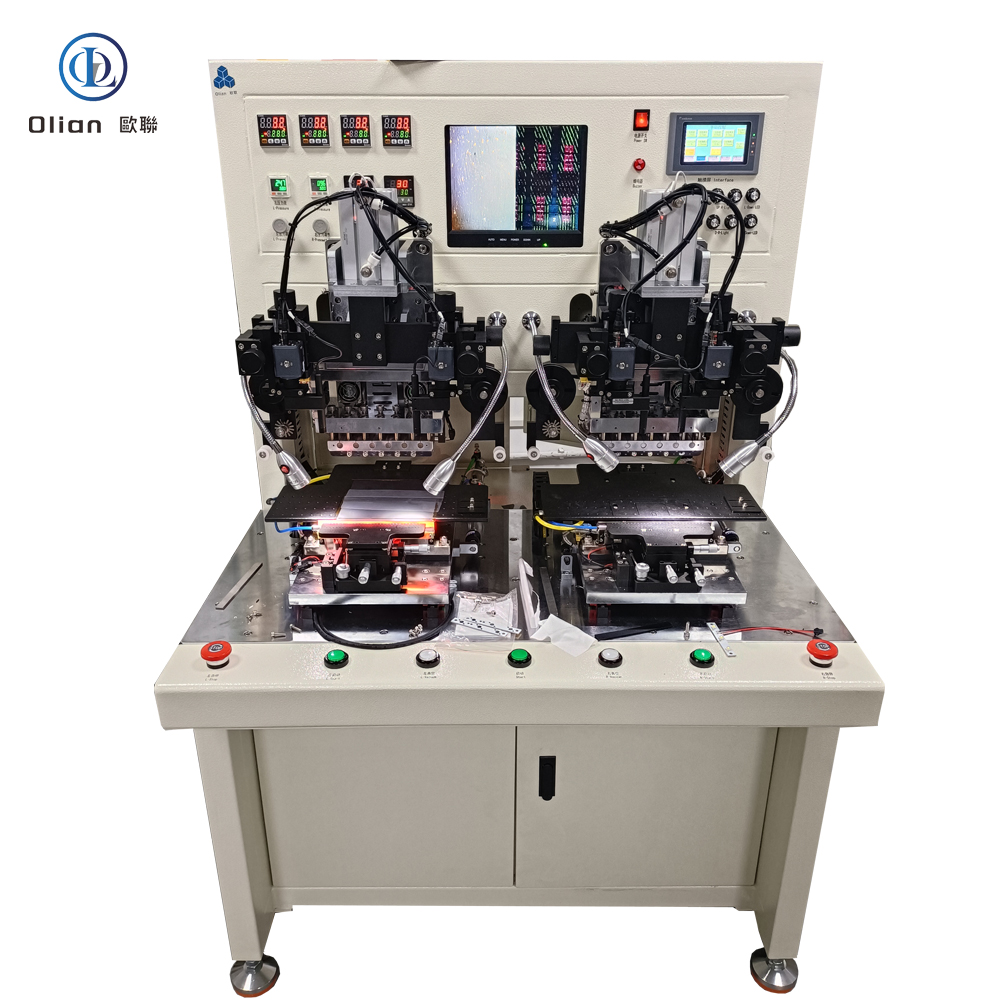
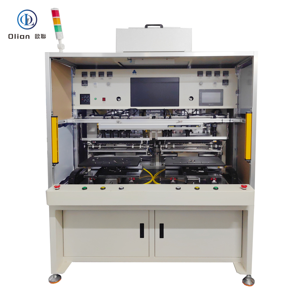

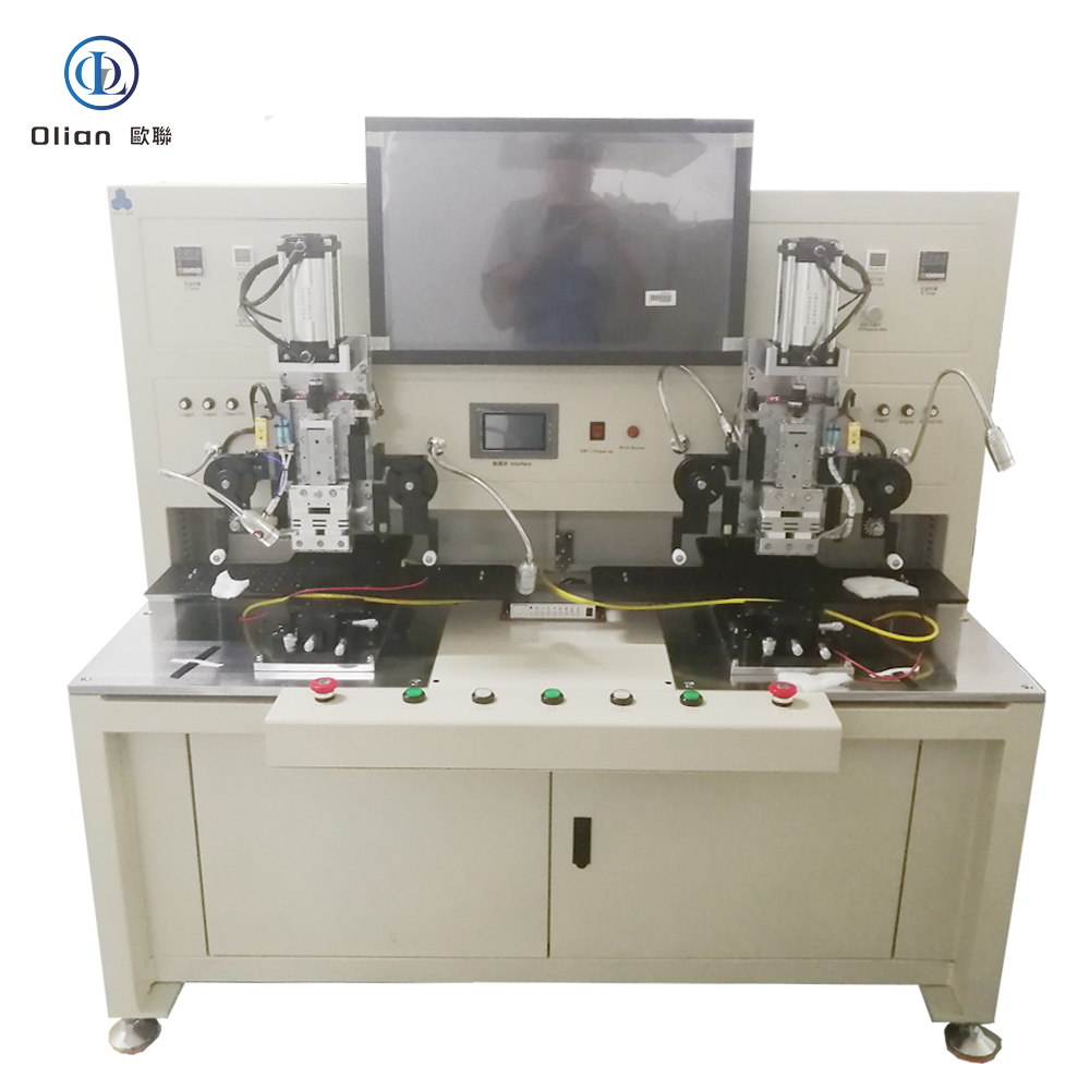
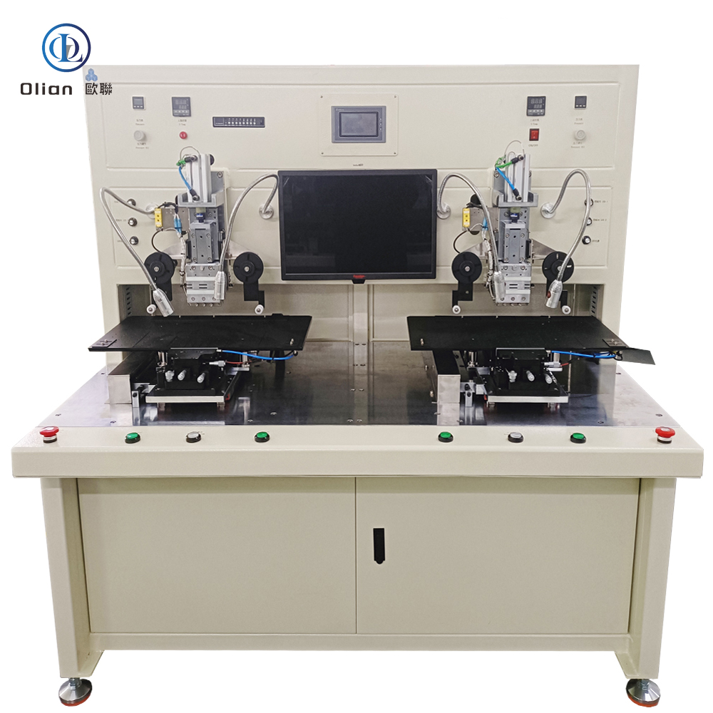
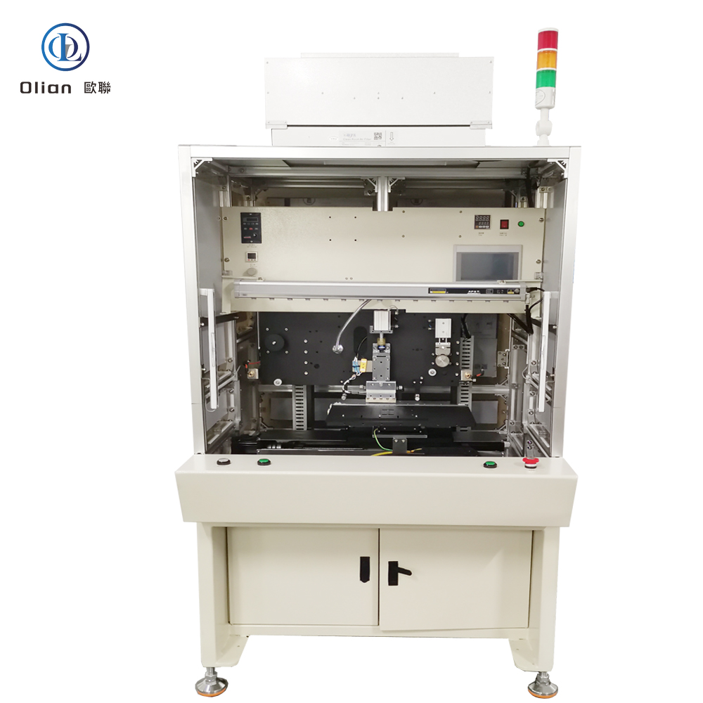
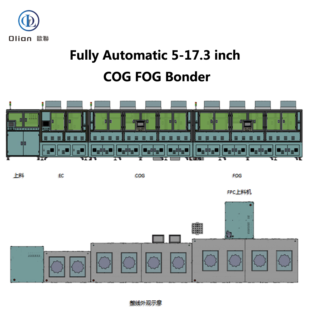
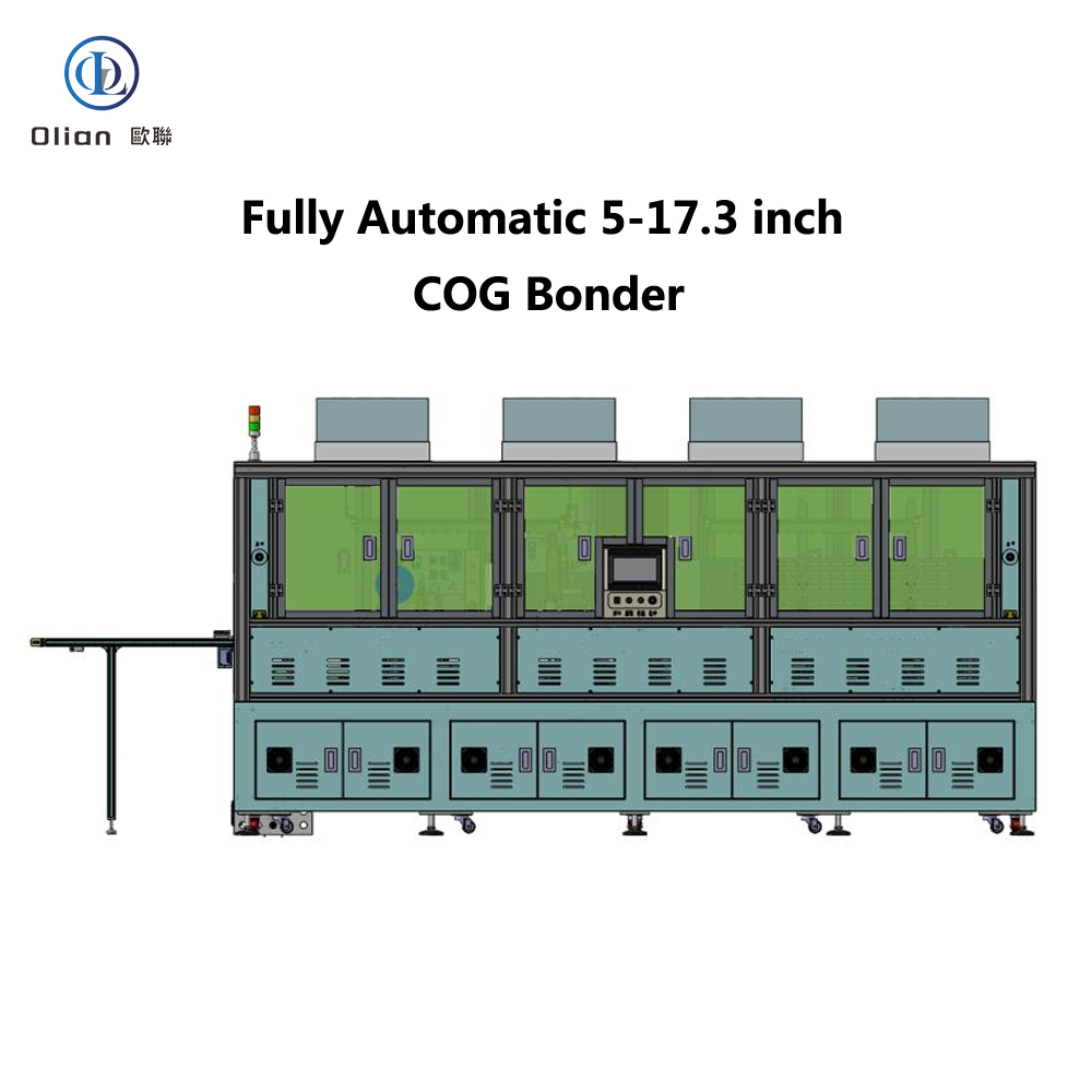
Electronic Paper Module Production Line: Precision Engineering for the Future of Low-Power DisplaysAs the global demand for energy-efficient, eye-friendly, and sustainable display technologies grows, electronic paper (e-Paper) has emerged as a transformative solution—powering devices such as e-readers, smart labels, digital signage, and IoT devices. At the heart of this innovation lies the Electronic Paper Module (EPM) Production Line, a highly specialized, precision-driven manufacturing system that integrates advanced automation, micro-assembly, and inspection technologies to deliver reliable, high-quality e-paper displays at scale.
An Electronic Paper Module (EPM) replicates the appearance of ink on paper by using electrophoretic or other reflective display technologies. Unlike traditional LCD or OLED screens, e-paper consumes power only when changing images, making it ideal for battery-powered and environmentally conscious applications.
The EPM typically consists of:
● Electronic Paper Film (EPD): The core display layer with microcapsules containing charged pigment particles.
● Thin-Film Transistor (TFT) Backplane: Controls pixel activation.
● Driver ICs and FPC (Flexible Printed Circuit): Deliver signals and power.
● Protective Front Film and Adhesive Layers: Ensure durability and optical clarity.
Manufacturing these modules requires a cleanroom-compatible, high-precision module production line capable of handling delicate materials and sub-micron alignment.
The EPM production line is a fully automated system designed to ensure high yield, consistency, and reliability. It integrates multiple advanced process modules, including:
● Automated cleaning removes dust and contaminants using brush, air-knife, and adhesive roller systems.
● Plasma treatment enhances surface adhesion for subsequent lamination processes.
● High-resolution CCD vision systems align the TFT backplane with the electronic paper film with accuracy within ±10μm.
● Active alignment compensates for thermal expansion and material warpage.
● Anisotropic Conductive Film (ACF) is precisely dispensed or laminated onto bonding areas.
● COG (Chip-on-Glass) or COF (Chip-on-Film) bonding connects driver ICs to the TFT array using thermocompression.
● Multi-point temperature and pressure control ensure reliable electrical connections without damaging fragile substrates.
● FPCs are bonded to the panel periphery for external signal routing.
● Robotic arms handle delicate modules to prevent mechanical stress.
● High-magnification cameras scan for defects such as particle contamination, alignment errors, open circuits, or short circuits.
● AI-powered image analysis enables real-time feedback and process correction.
● Modules undergo accelerated aging under controlled temperature and voltage to stabilize performance.
● Electrical testing verifies grayscale response, refresh rate, and power consumption.
● Qualified modules are automatically packed in anti-static, humidity-controlled packaging.
● Traceability systems record production data for quality tracking.
● Ultra-Clean Environment Compatibility: Designed for Class 100–1000 cleanrooms to prevent particle-induced defects.
● High Precision & Repeatability: Sub-pixel alignment ensures uniform image quality.
● Low Particle Generation: Use of non-contact handling and low-outgassing materials.
● Flexible Configuration: Supports various sizes (from 1.5” e-readers to 25” digital signage) and backplane technologies (a-Si, IGZO, LTPS).
● Smart Manufacturing Integration: Equipped with SECS/GEM, MES, and SCADA systems for real-time monitoring, data analytics, and predictive maintenance.
● Energy Efficiency: Optimized thermal management and low-power consumption design align with e-paper’s green philosophy.
● E-Readers (e.g., Kindle, Kobo): High-resolution, glare-free reading experience.
● Retail Smart Labels: Wireless, updateable price tags reducing labor and paper waste.
● Public Information Displays: Bus stops, train stations with sunlight-readable screens.
● Medical Devices: Low-power patient monitors and electronic charts.
● Smart Home & IoT: Battery-operated sensors and control panels.
At Olian Automatic, we specialize in designing and delivering turnkey Electronic Paper Module Production Lines that combine precision, reliability, and intelligence. Our solutions are built on decades of expertise in module assembly, bonding technology, and smart factory integration.
Our EPM production systems feature:
● Proprietary alignment and bonding algorithms
● Modular design for rapid reconfiguration
● Integrated AI-based defect detection
● End-to-end process support—from dispensing to aging
● Global service and technical support network
We partner with leading e-paper manufacturers and material suppliers to ensure compatibility with the latest EPD films, ACF materials, and driver ICs.
As e-paper technology evolves—enabling color displays, faster refresh rates, and flexible form factors—the production line must keep pace. Emerging trends include:
● Roll-to-Roll (R2R) Processing: For high-speed, low-cost manufacturing of flexible e-paper.
● Hybrid Backplanes: Combining IGZO with organic semiconductors for improved performance.
● Miniaturization and Integration: Smaller modules for wearable and medical devices.
● Sustainable Manufacturing: Reduced chemical usage, recyclable materials, and energy-efficient processes.
The Electronic Paper Module Production Line will continue to be a cornerstone of this evolution, bridging innovation and industrialization.
The Electronic Paper Module Production Line represents the convergence of precision engineering, automation, and sustainable technology. As the world shifts toward low-power, human-centric displays, manufacturers need intelligent, flexible, and future-ready solutions.
With Olian Automatic’s comprehensive portfolio of bonding machines, module lines, and smart factory systems, we are committed to empowering the next generation of e-paper innovation—delivering clarity, efficiency, and value to our customers worldwide.
Olian Automatic – Precision. Intelligence. Innovation. Empowering the Future of Displays.
Electronic Paper Module, EPM Production Line, e-Paper Manufacturing, Electrophoretic Display, TFT Backplane, COG Bonding, COF Bonding, ACF Lamination, Automated Optical Inspection, AOI, Flexible Printed Circuit, FPC, Driver IC, Module Assembly, Cleanroom Manufacturing, Precision Alignment, Vision System, Smart Factory, SECS/GEM, MES, SCADA, Low-Power Display, Reflective Display, IoT Devices, Digital Signage, Retail Smart Labels, E-Readers
Tags: e-Paper, Module Production, Display Technology, Automation, Precision Engineering, Manufacturing Line, Semiconductor Packaging, Bonding Process, Quality Control, AOI, Cleanroom, Flexible Electronics, IoT, Digital Transformation, Sustainable Display
Please contact us wechat/whatsapp:+86 18025364779 Zack wu