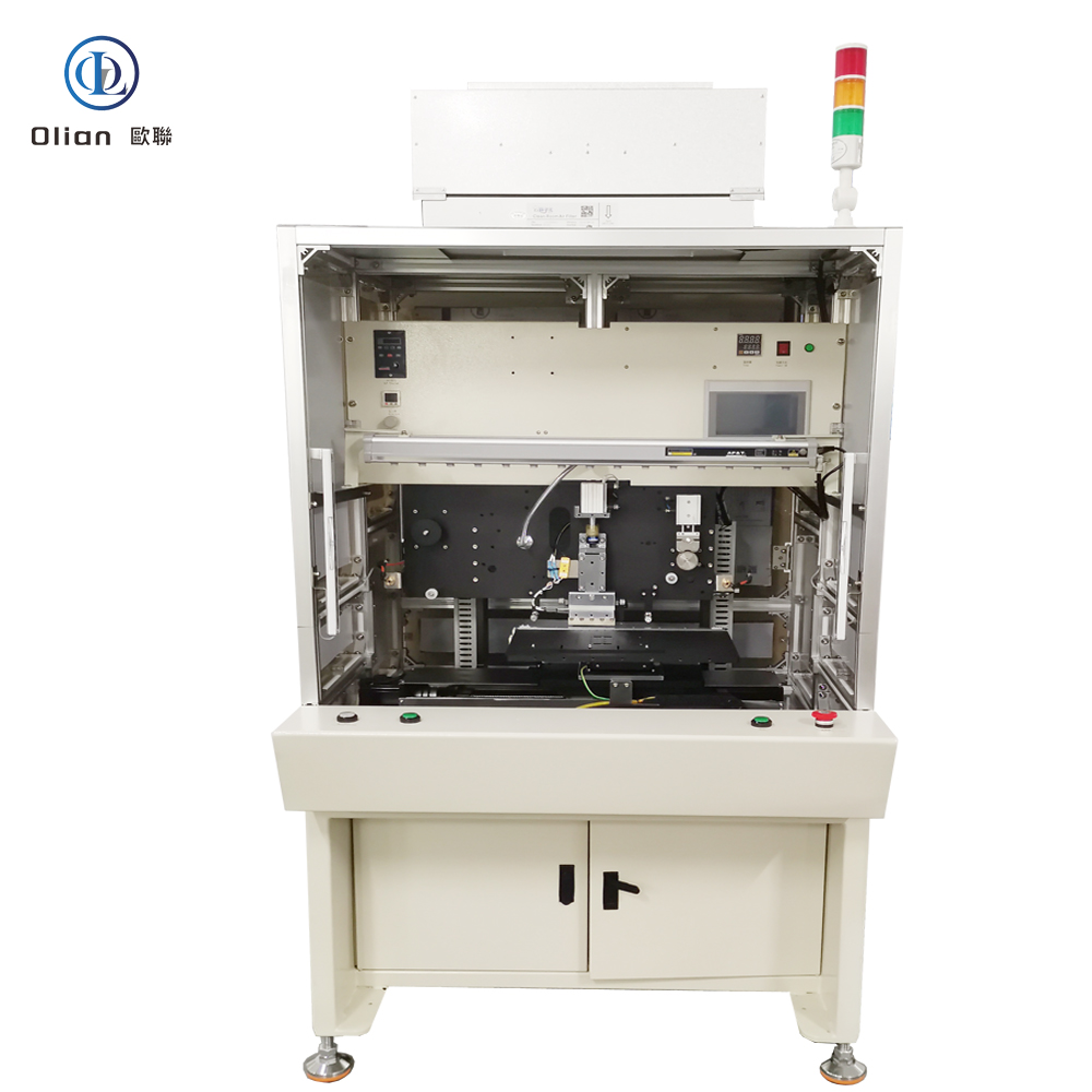
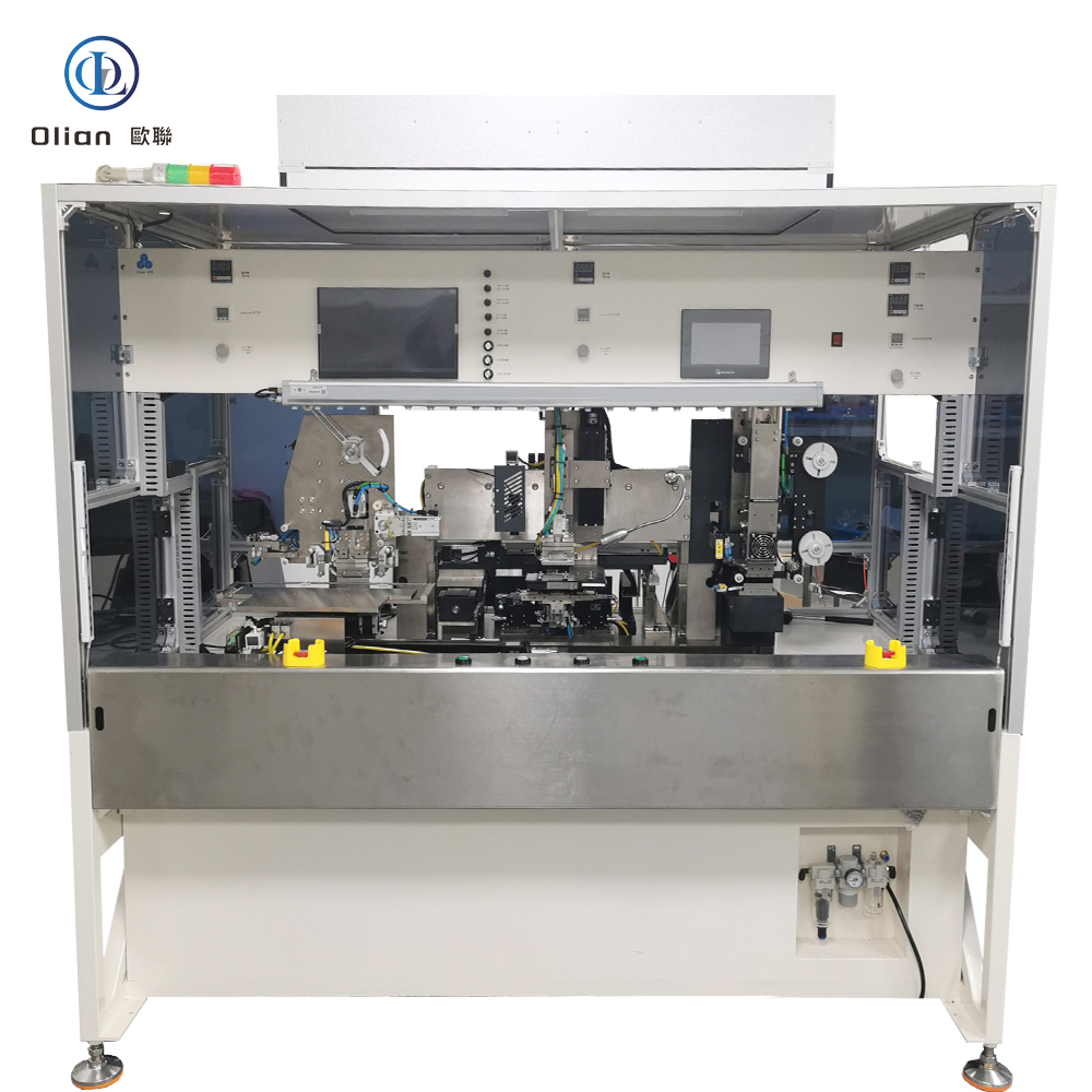
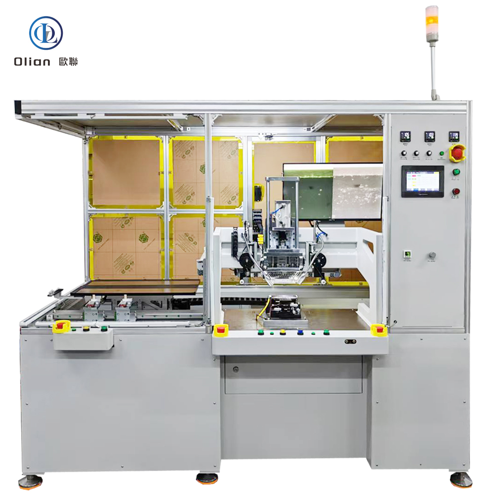
Flexible Display Module Bonding Equipment: Precision Engineering for Next-Gen Wearables and Smart Devices.
Flexible Display Module Bonding Equipment
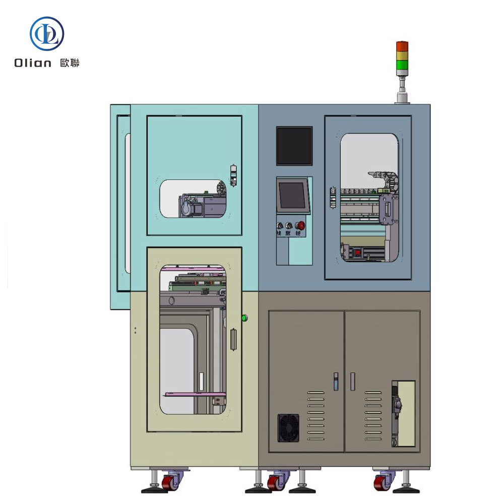
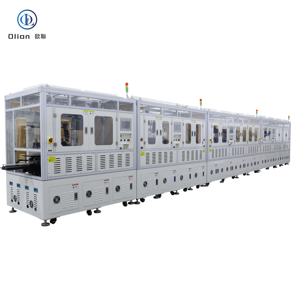
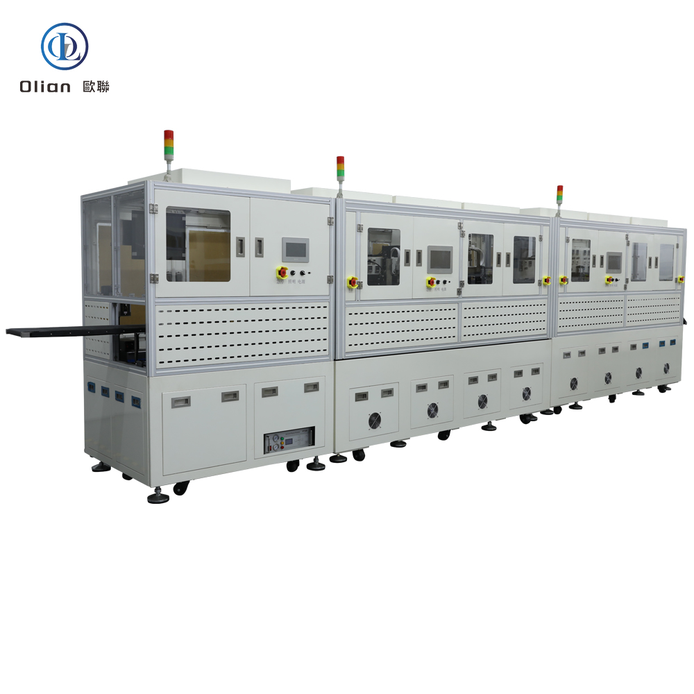
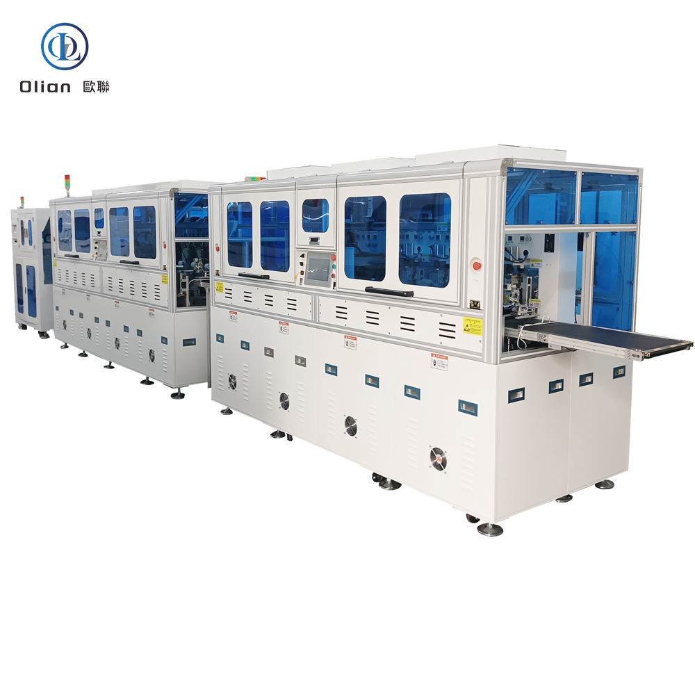
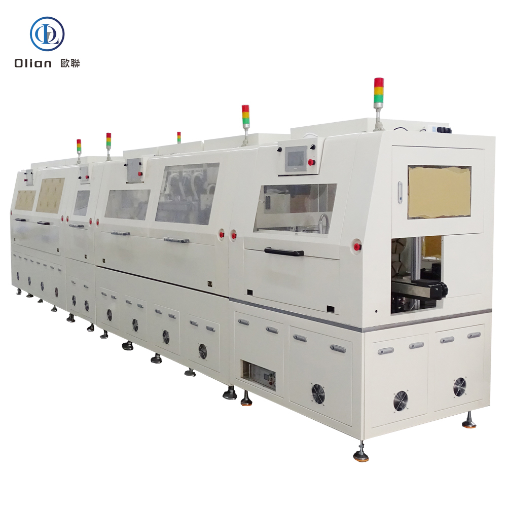
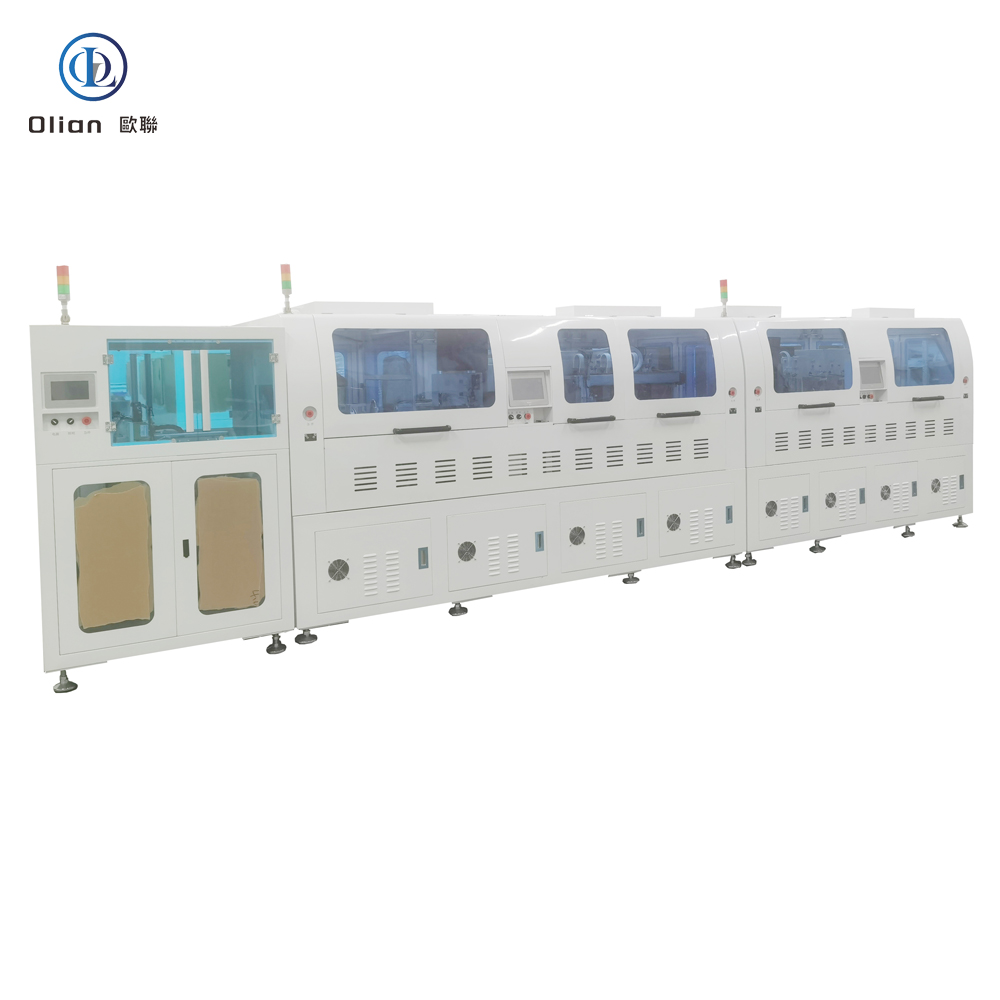
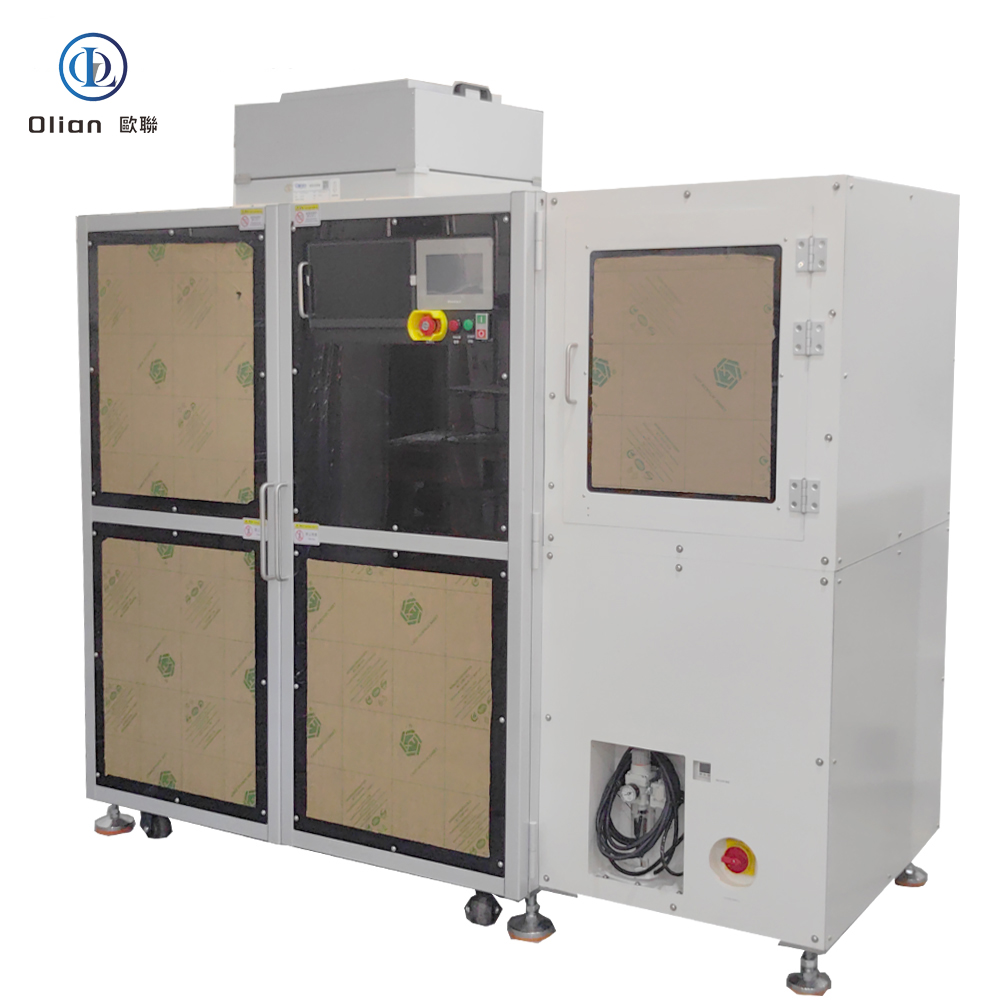
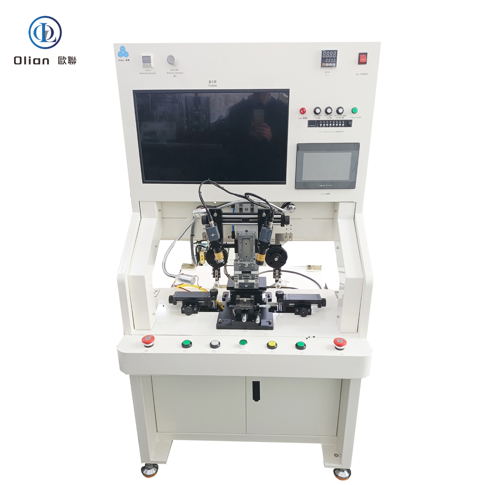
As the demand for flexible electronics surges across industries—from smartwatches and foldable smartphones to wearable health monitors and AR/VR devices—the manufacturing of flexible display modules has become a cornerstone of modern electronics production. At the heart of this revolution lies the Flexible Display Module Bonding Equipment, a highly advanced, precision-driven system engineered to deliver reliable, high-yield interconnections between delicate flexible displays and their driving circuitry.
This specialized equipment plays a critical role in the assembly of flexible OLED, micro-LED, and e-paper modules, ensuring robust electrical connections while maintaining the mechanical flexibility and durability essential for next-generation devices. Among the key bonding technologies, COP (Chip on Plastic) and FOP (FPC on Plastic) have emerged as pivotal processes, especially for ultra-compact and curved wearable displays, enabling innovative form factors and enhanced integration.
What is Flexible Display Module Bonding?
Module bonding refers to the process of connecting the display panel (typically a flexible substrate) with driver ICs (Integrated Circuits) and Flexible Printed Circuits (FPCs). In flexible displays, this process must accommodate ultra-thin, bendable materials without compromising electrical performance or structural integrity.
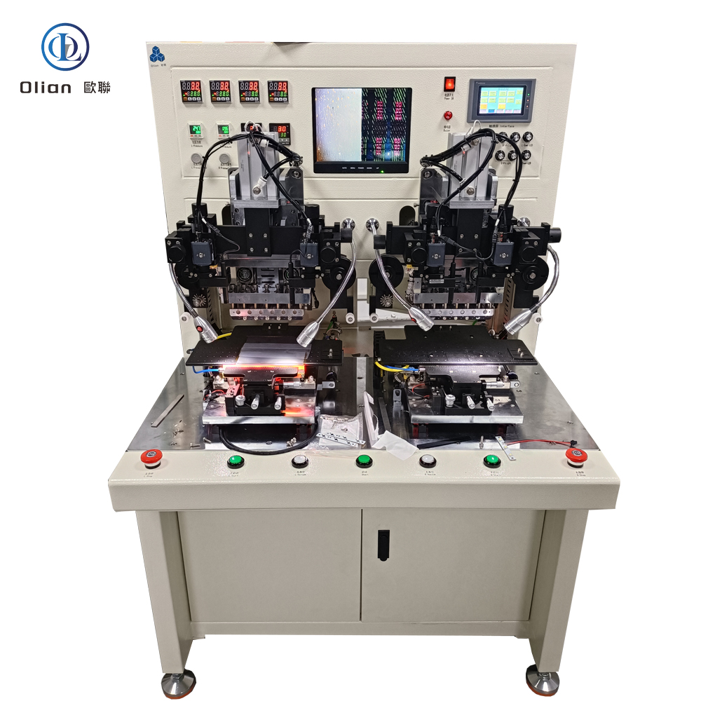
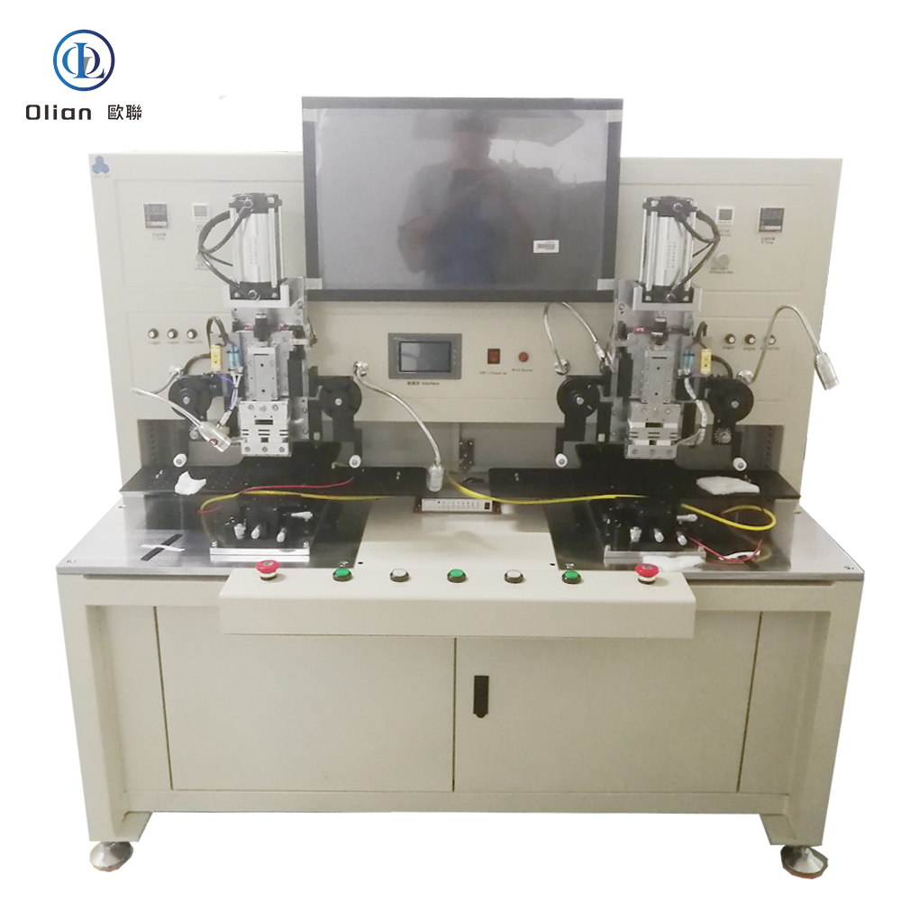
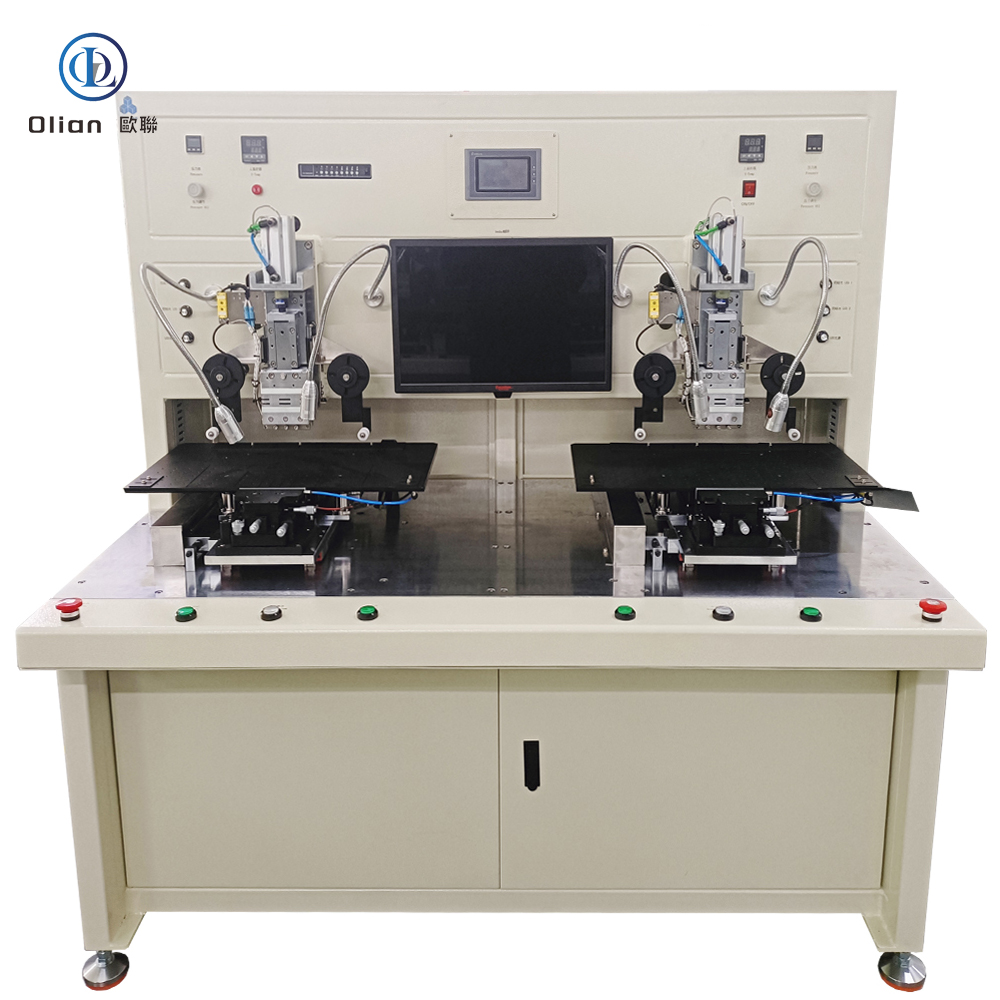
The Flexible Display Module Bonding Equipment performs key processes such as Chip-on-Film (COF), Tape Automated Bonding (TAB), and increasingly, COP (Chip on Plastic) and FOP (FPC on Plastic), enabling high-density, fine-pitch interconnections directly onto plastic or flexible substrates—eliminating the need for rigid carriers and enabling true flexibility.
Core Processes and Technologies
1. Chip-on-Plastic (COP) Bonding
● Definition: COP refers to the direct bonding of a bare Integrated Circuit (IC) onto a plastic-based flexible substrate (such as PI—Polyimide), typically at the edge of the display panel.
● Process Flow: ACF is pre-laminated on the bonding area; the bare IC is precisely aligned and placed; Thermocompression bonding forms the connection.
● Advantages: Enables ultra-narrow bezel design, reduces thickness, and maintains high flexibility.
● Applications: Smartwatches, AR glasses, and ultra-thin fitness bands.
2. FPC-on-Plastic (FOP) Bonding
● Definition: FOP involves bonding a Flexible Printed Circuit (FPC) directly onto a plastic substrate of the display module.
● Process Flow: ACF is applied; the FPC tip is aligned and bonded using thermocompression.
● Advantages: Offers enhanced design freedom for 3D shaping and ensures robust mechanical connections resistant to bending fatigue.
● Applications: Foldable phones, curved automotive displays, and wearable medical devices.
3. Chip-on-Film (COF) Bonding
● Mounts driver ICs on a flexible polyimide (PI) film carrier, which is then bonded to the display panel using ACF. Offers excellent flexibility for high-end displays.
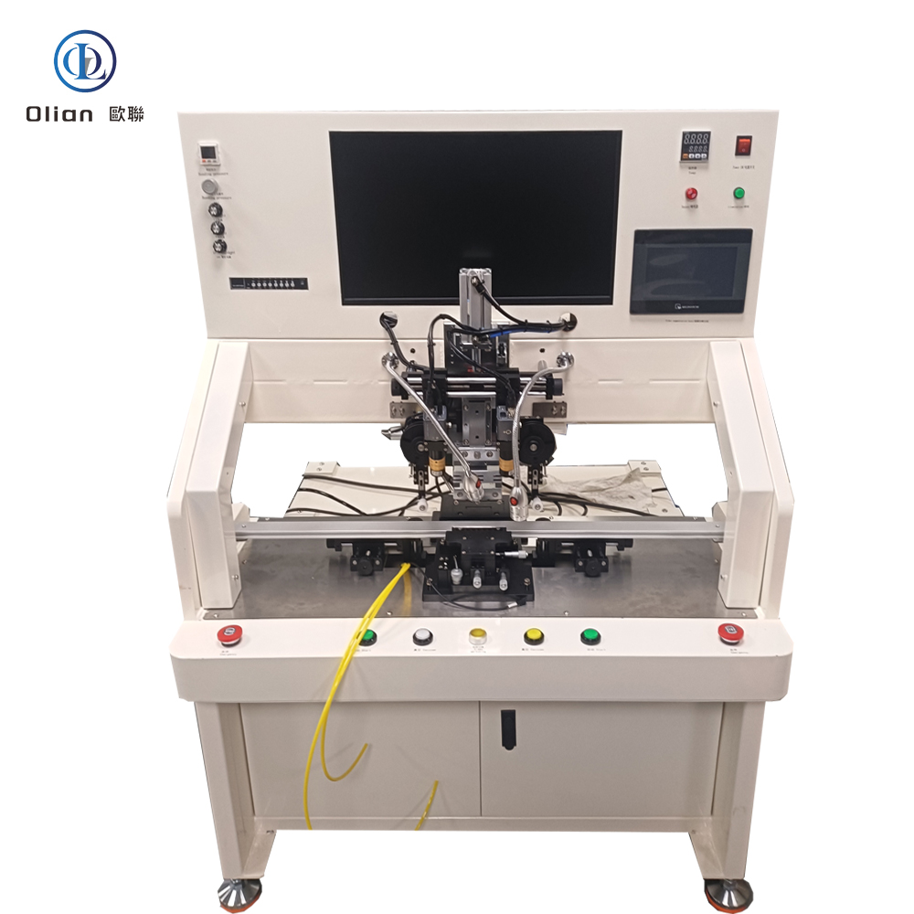
4. Fine-Pitch Alignment and Placement
● Equipped with high-resolution vision systems and nano-positioning stages to achieve alignment accuracy within ±3–5μm, essential for COP and FOP processes.
5. Thermocompression Bonding
● Utilizes multi-zone heating heads to ensure uniform temperature distribution and programmable force profiles for different materials.
6. Post-Bonding Inspection and Testing
● Integrated AOI (Automated Optical Inspection) detects misalignment, ACF voids, or IC tilt, ensuring high yield.
Key Features of Advanced COP/FOP Bonding Equipment
● COP & FOP Process Optimization: Dedicated tooling for direct bonding on plastic substrates.
● Ultra-Fine Pitch Capability: Supports pitch down to 20μm.
● Low Thermal Budget: Prevents warping of sensitive plastic substrates.
● 3D Surface Bonding: Adaptive pressure for curved and non-planar surfaces.
● Smart Process Control: Real-time monitoring via MES integration and predictive maintenance.
Why COP and FOP Are Game-Changers
These processes enable True Flexibility and Miniaturization, which are critical for wearables. By bonding directly on plastic, they eliminate rigid carriers, allowing displays to bend and fold seamlessly.
Olian Automatic: Pioneering COP and FOP Bonding Solutions
At Olian Automatic, we are at the forefront of developing next-generation COP and FOP bonding equipment tailored for the future of flexible electronics. Our systems integrate advanced vision alignment, adaptive thermocompression, and intelligent process control to deliver unmatched precision and yield.
We understand that COP and FOP are not just processes—they are enablers of innovation. That’s why our equipment is designed with modularity, scalability, and ease of integration in mind, supporting customers from R&D to mass production.
With deep expertise in ACF handling, ultra-fine pitch bonding, and flexible substrate processing, Olian Automatic empowers manufacturers to push the boundaries of what’s possible in wearable and flexible display technology.
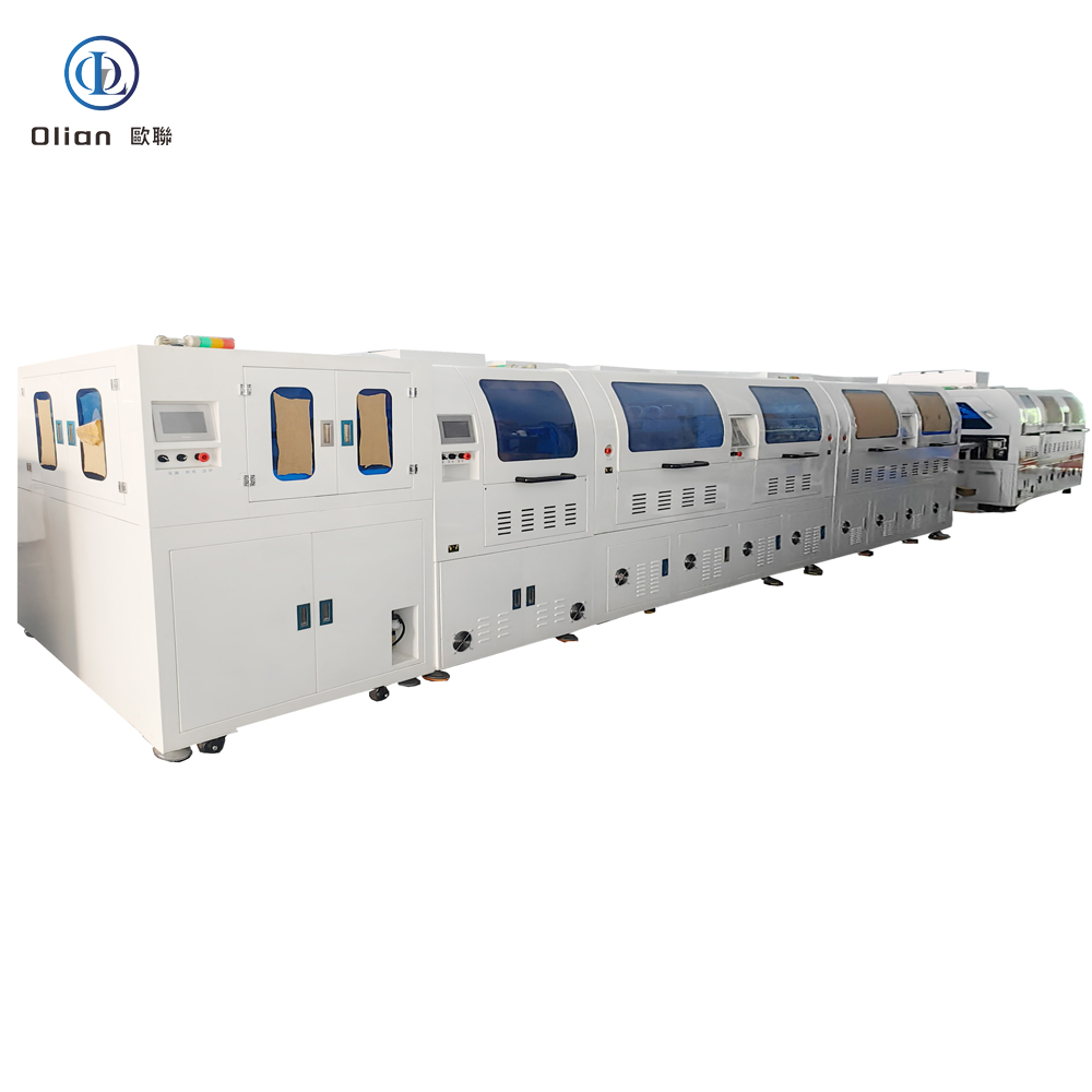
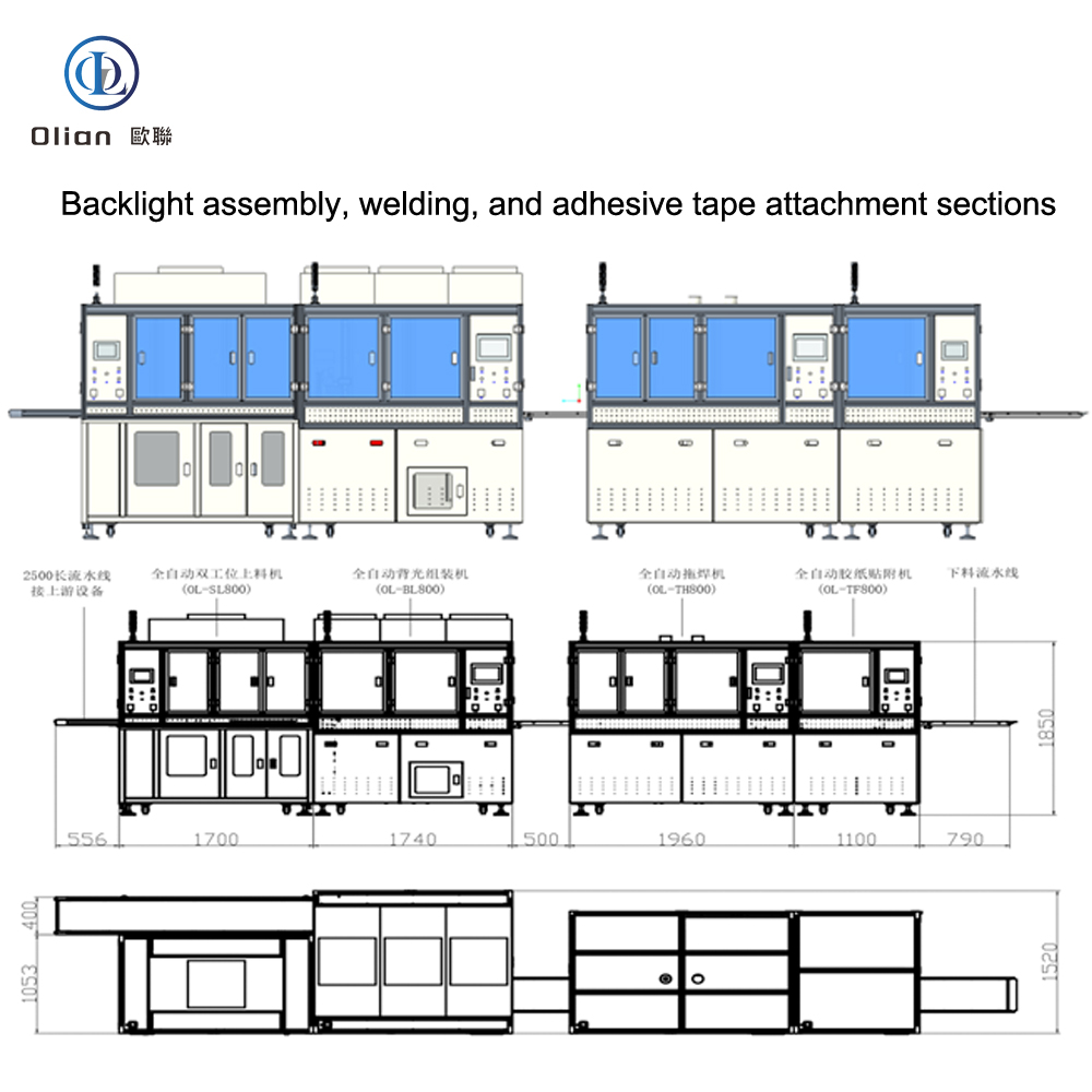
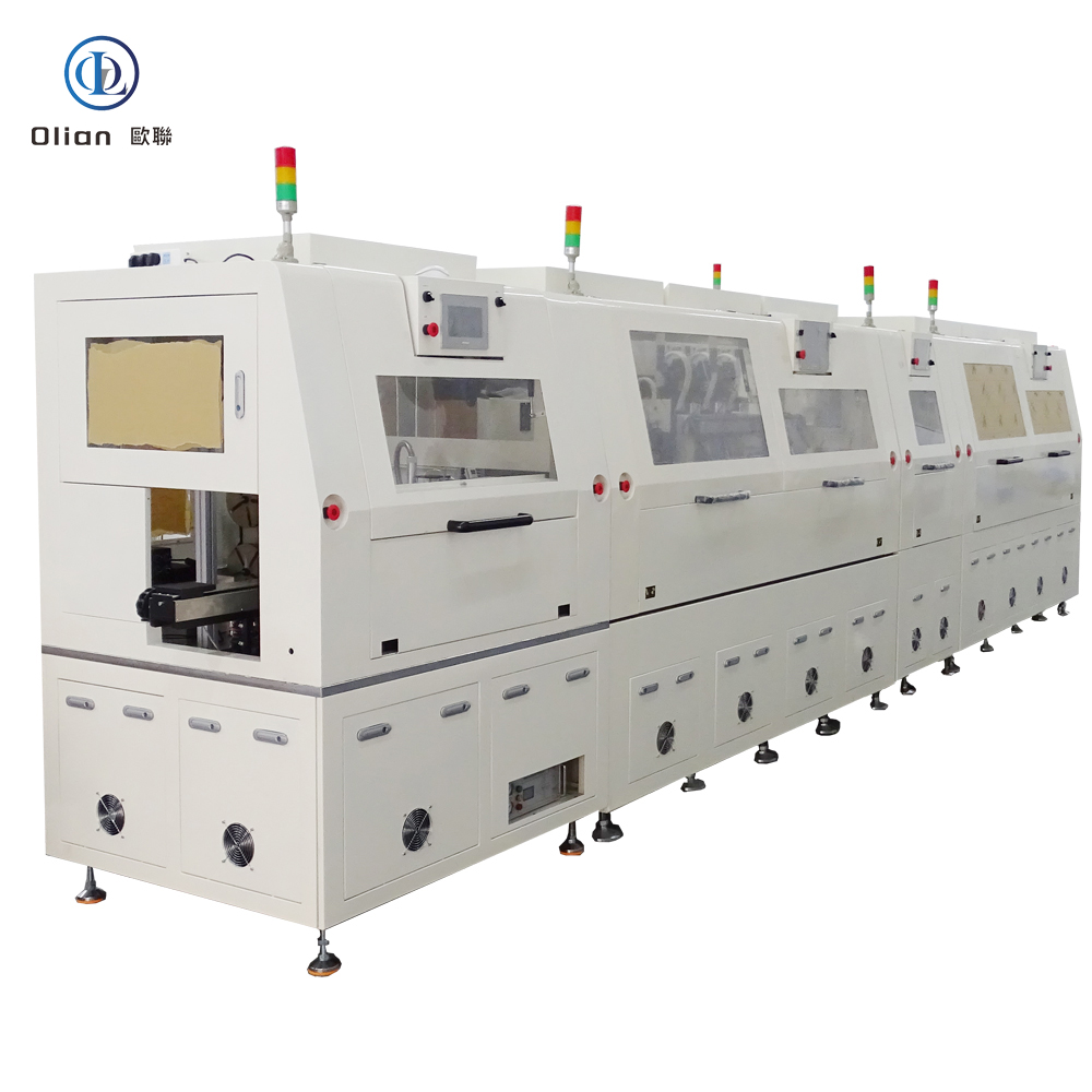
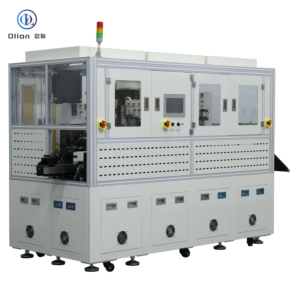
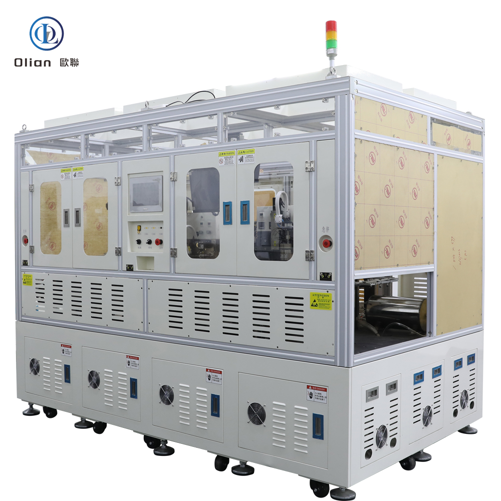
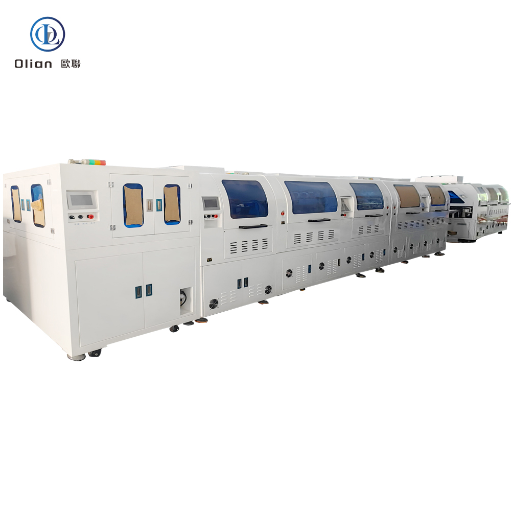
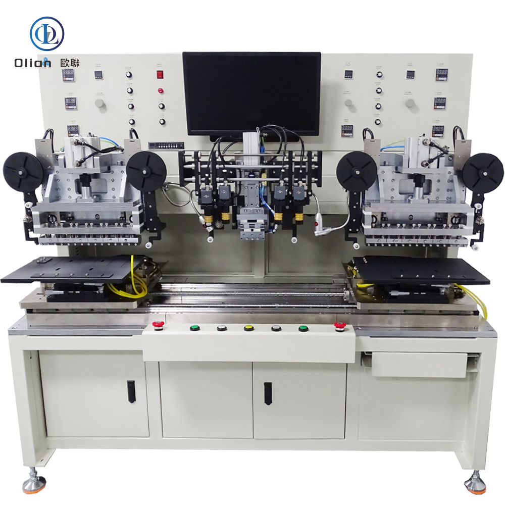
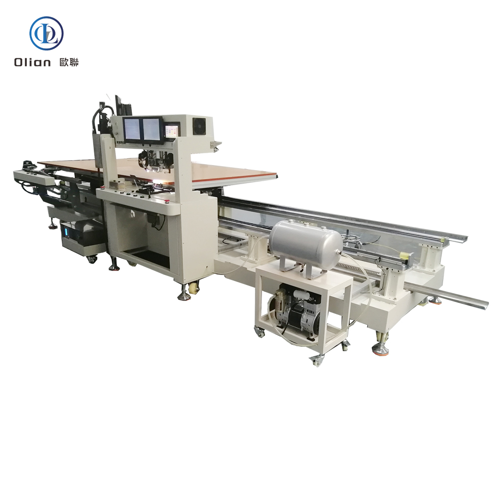
Wearable Device Display Manufacturing Line: Enabling the Future of Compact, Flexible, and High-Performance Wearables
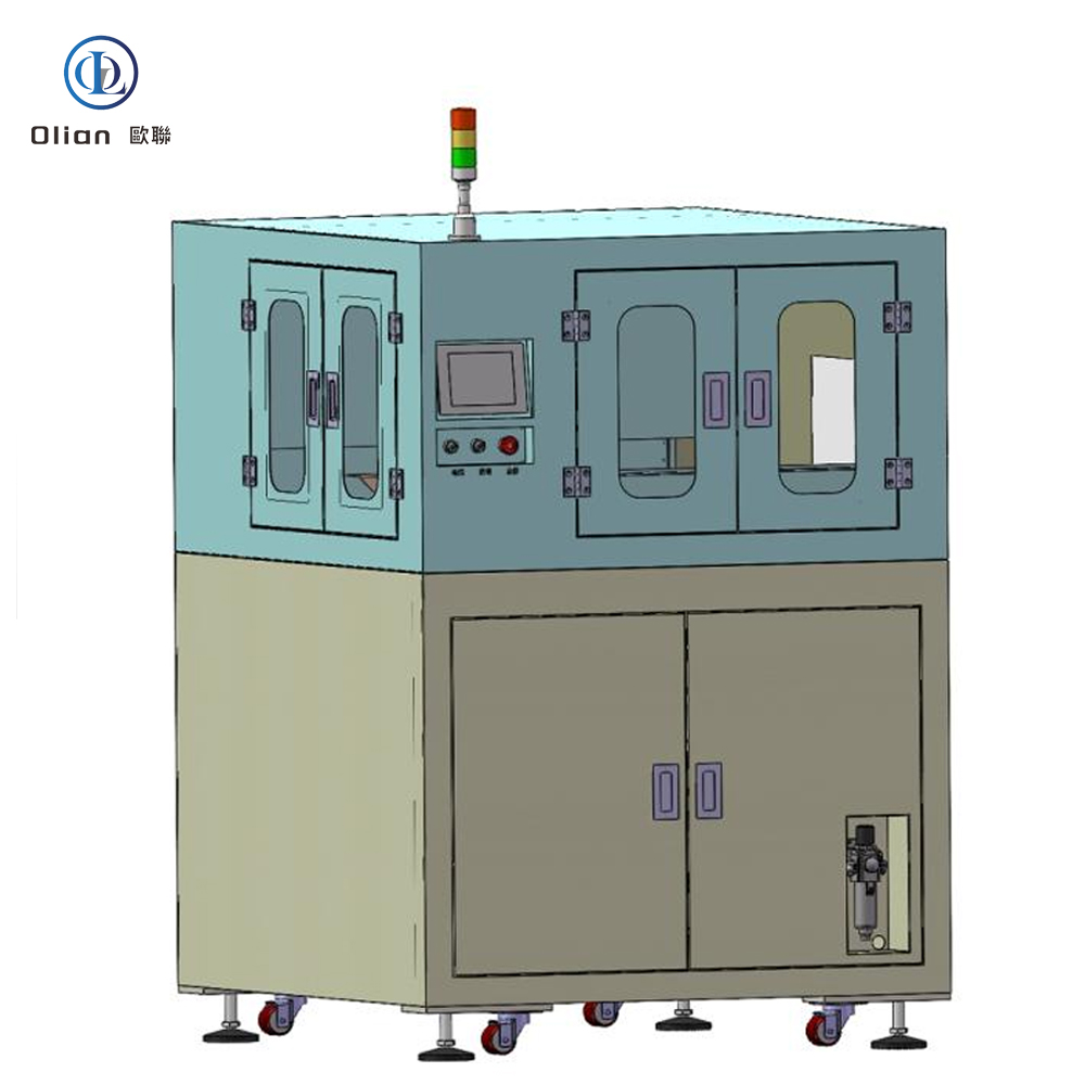
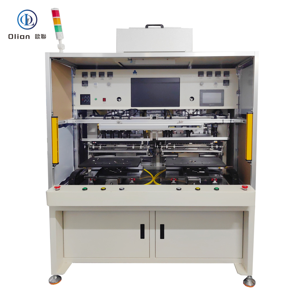
As wearable technology continues to evolve—from smartwatches and fitness trackers to AR glasses and health monitoring patches—the demand for compact, durable, flexible, and energy-efficient displays has surged. At the core of this innovation lies the Wearable Device Display Manufacturing Line, a highly sophisticated, precision-driven production system engineered to meet the unique challenges of small-form-factor, curved, and often flexible displays used in modern wearables.
This advanced manufacturing line integrates cutting-edge automation, micro-assembly technologies, and stringent quality control systems to deliver high-yield, reliable, and aesthetically pleasing displays that seamlessly blend form and function.
The Evolution of Wearable Displays
Wearable devices require displays that are not only visually clear and responsive but also lightweight, power-efficient, and mechanically robust. Traditional rigid displays are increasingly being replaced by flexible OLED, micro-LED, and even electronic paper (e-Paper) technologies that conform to the human body and withstand constant movement and environmental stress.
The Wearable Device Display Manufacturing Line is specifically designed to handle these advanced display types, supporting both rigid and flexible substrates, ultra-thin components, and miniaturized packaging.
Key Components of the Wearable Display Manufacturing Line
1. Cleanroom-Compatible Automation
○ Operates in Class 100–1000 cleanrooms to prevent particle contamination.
○ Robotic arms with nano-precision handling ensure safe transfer of fragile display panels.
● Smart Manufacturing Integration: Fully compatible with SECS/GEM, MES, and IoT platforms for real-time monitoring, traceability, and predictive maintenance.
● Energy and Material Efficiency: Optimized processes reduce waste and power consumption, aligning with sustainable manufacturing goals.
● Scalability: Designed for both high-volume mass production and small-batch customization.
Olian Automatic: Pioneering the Future of Wearable Display Manufacturing
At Olian Automatic, we specialize in designing and delivering turnkey Wearable Device Display Manufacturing Lines that combine precision, reliability, and intelligence. Our solutions are built to support the rapid innovation cycles of the wearable industry, enabling manufacturers to bring next-generation products to market faster, with higher quality and lower total cost of ownership.
From concept to full-scale production, our engineering team works closely with clients to customize workflows, integrate advanced inspection systems, and ensure seamless compatibility with existing production ecosystems.
Welcome to visit us ,Wechat/whatsapp:+86 18025364779,Zack wu
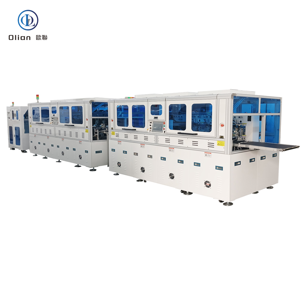
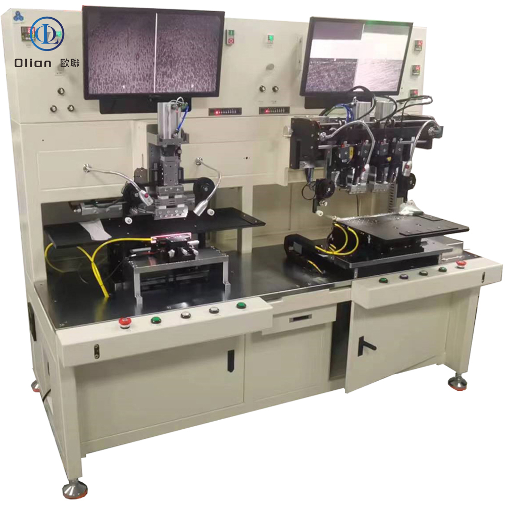
Electronic Paper Module Production Line: Precision Engineering for the Future of Low-Power Displays.
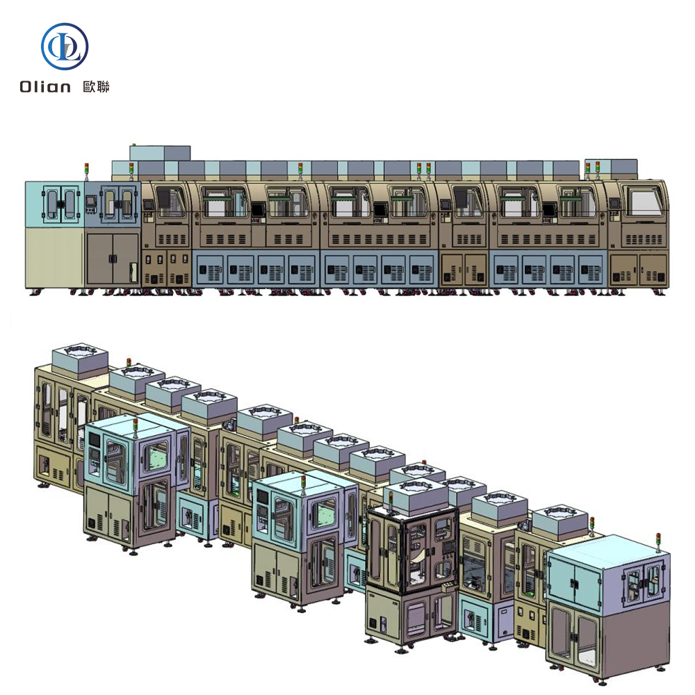
Electronic Paper Module Production Line: Precision Engineering for the Future of Low-Power DisplaysAs the global demand for energy-efficient, eye-friendly, and sustainable display technologies grows, electronic paper (e-Paper) has emerged as a transformative solution—powering devices such as e-readers, smart labels, digital signage, and IoT devices. At the heart of this innovation lies the Electronic Paper Module (EPM) Production Line, a highly specialized, precision-driven manufacturing system that integrates advanced automation, micro-assembly, and inspection technologies to deliver reliable, high-quality e-paper displays at scale.
What Is an Electronic Paper Module?
An Electronic Paper Module (EPM) replicates the appearance of ink on paper by using electrophoretic or other reflective display technologies. Unlike traditional LCD or OLED screens, e-paper consumes power only when changing images, making it ideal for battery-powered and environmentally conscious applications.
The EPM typically consists of:
● Electronic Paper Film (EPD): The core display layer with microcapsules containing charged pigment particles.
● Driver ICs and FPC (Flexible Printed Circuit): Deliver signals and power.
● Protective Front Film and Adhesive Layers: Ensure durability and optical clarity.
Manufacturing these modules requires a cleanroom-compatible, high-precision module production line capable of handling delicate materials and sub-micron alignment.
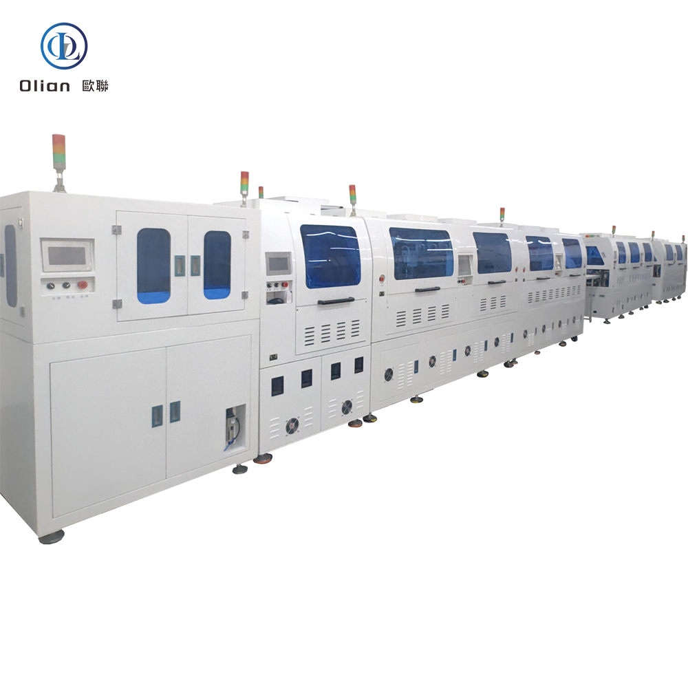
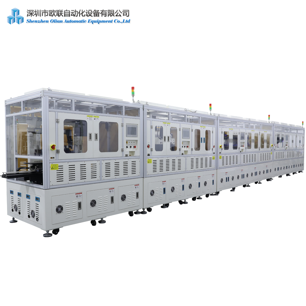
The Electronic Paper Module Production Line: A Comprehensive Workflow
The EPM production line is a fully automated system designed to ensure high yield, consistency, and reliability. It integrates multiple advanced process modules, including:
1. Panel Cleaning and Pre-treatment
● Automated cleaning removes dust and contaminants using brush, air-knife, and adhesive roller systems.
● Plasma treatment enhances surface adhesion for subsequent lamination processes.
2. TFT Backplane and EPD Alignment
● High-resolution CCD vision systems align the TFT backplane with the electronic paper film with accuracy within ±10μm.
● Active alignment compensates for thermal expansion and material warpage.
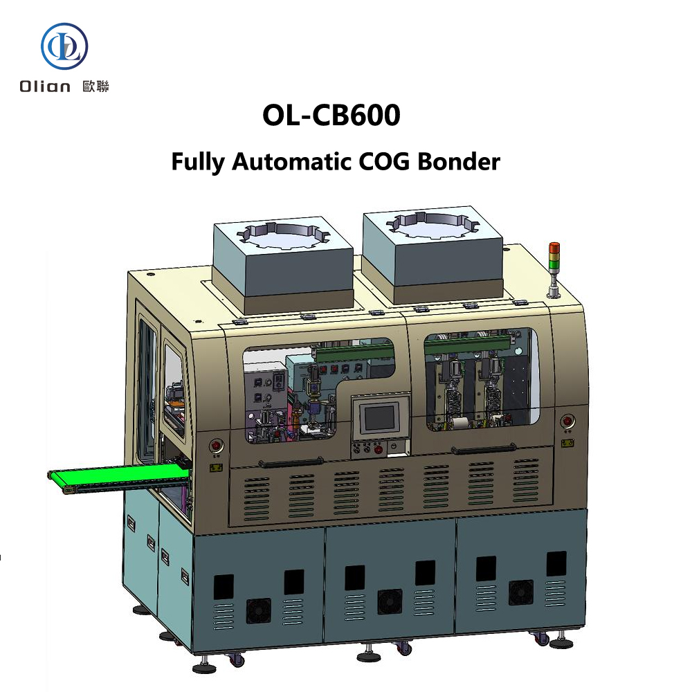
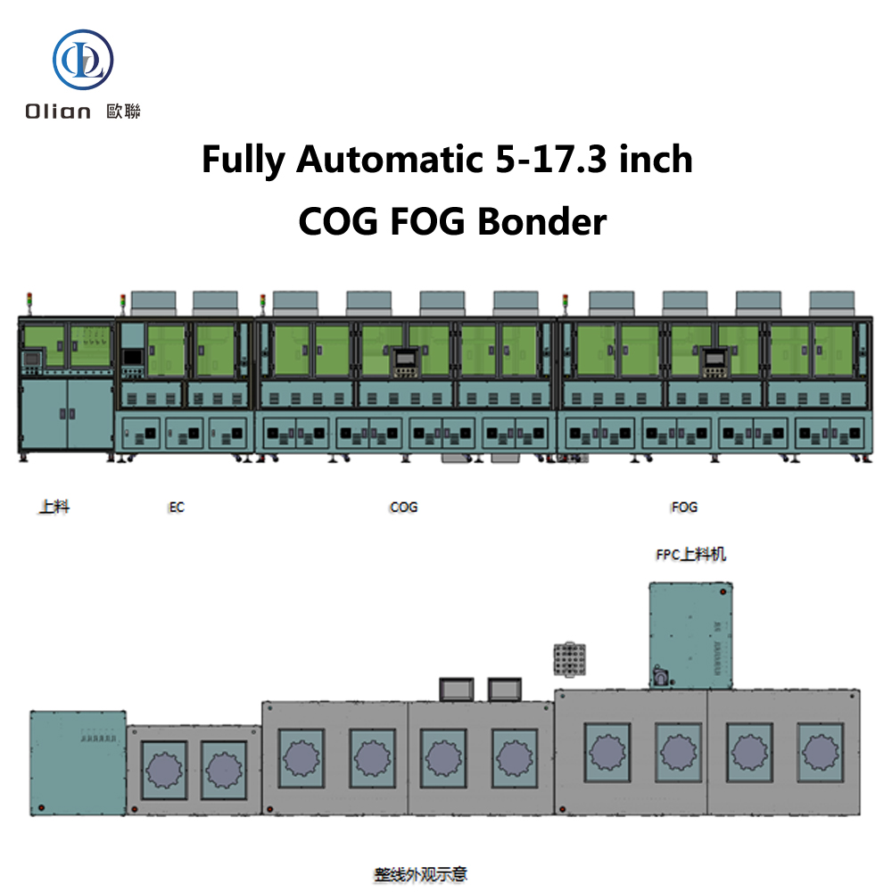
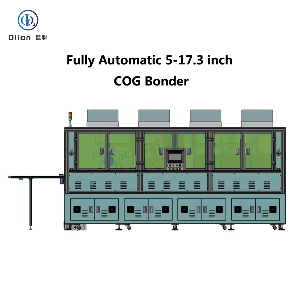
3. ACF Lamination and COG/COF Bonding
● Anisotropic Conductive Film (ACF) is precisely dispensed or laminated onto bonding areas.
● COG (Chip-on-Glass) or COF (Chip-on-Film) bonding connects driver ICs to the TFT array using thermocompression.
● Multi-point temperature and pressure control ensure reliable electrical connections without damaging fragile substrates.
4. FPC Attachment and Module Assembly
● FPCs are bonded to the panel periphery for external signal routing.
● Robotic arms handle delicate modules to prevent mechanical stress.
5. Automated Optical Inspection (AOI) and M/A Detection
● High-magnification cameras scan for defects such as particle contamination, alignment errors, open circuits, or short circuits.
● AI-powered image analysis enables real-time feedback and process correction.
6. Aging and Functional Testing
● Modules undergo accelerated aging under controlled temperature and voltage to stabilize performance.
● Electrical testing verifies grayscale response, refresh rate, and power consumption.
7. Packing and Final QC
● Qualified modules are automatically packed in anti-static, humidity-controlled packaging.
● Traceability systems record production data for quality tracking.
Key Features of a Modern EPM Production Line
● Ultra-Clean Environment Compatibility: Designed for Class 100–1000 cleanrooms to prevent particle-induced defects.
● Low Particle Generation: Use of non-contact handling and low-outgassing materials.
● Flexible Configuration: Supports various sizes (from 1.5” e-readers to 25” digital signage) and backplane technologies (a-Si, IGZO, LTPS).
● Smart Manufacturing Integration: Equipped with SECS/GEM, MES, and SCADA systems for real-time monitoring, data analytics, and predictive maintenance.
● Energy Efficiency: Optimized thermal management and low-power consumption design align with e-paper’s green philosophy.
● Retail Smart Labels: Wireless, updateable price tags reducing labor and paper waste.
● Public Information Displays: Bus stops, train stations with sunlight-readable screens.
● Medical Devices: Low-power patient monitors and electronic charts.
● Smart Home & IoT: Battery-operated sensors and control panels.
Olian Automatic: Leading the EPM Manufacturing Revolution
At Olian Automatic, we specialize in designing and delivering turnkey Electronic Paper Module Production Lines that combine precision, reliability, and intelligence. Our solutions are built on decades of expertise in module assembly, bonding technology, and smart factory integration.
Our EPM production systems feature:
● Proprietary alignment and bonding algorithms
● Modular design for rapid reconfiguration
● Integrated AI-based defect detection
● End-to-end process support—from dispensing to aging
● Global service and technical support network
We partner with leading e-paper manufacturers and material suppliers to ensure compatibility with the latest EPD films, ACF materials, and driver ICs.
The Future of EPM Manufacturing
As e-paper technology evolves—enabling color displays, faster refresh rates, and flexible form factors—the production line must keep pace. Emerging trends include:
● Roll-to-Roll (R2R) Processing: For high-speed, low-cost manufacturing of flexible e-paper.
● Hybrid Backplanes: Combining IGZO with organic semiconductors for improved performance.
● Miniaturization and Integration: Smaller modules for wearable and medical devices.
● Sustainable Manufacturing: Reduced chemical usage, recyclable materials, and energy-efficient processes.
The Electronic Paper Module Production Line will continue to be a cornerstone of this evolution, bridging innovation and industrialization.
Conclusion
The Electronic Paper Module Production Line represents the convergence of precision engineering, automation, and sustainable technology. As the world shifts toward low-power, human-centric displays, manufacturers need intelligent, flexible, and future-ready solutions.
With Olian Automatic’s comprehensive portfolio of bonding machines, module lines, and smart factory systems, we are committed to empowering the next generation of e-paper innovation—delivering clarity, efficiency, and value to our customers worldwide.
Olian Automatic – Precision. Intelligence. Innovation. Empowering the Future of Displays.
Shenzhen Olian Automatic Equipment Co.,ltd .We are a leading high-tech enterprise dedicated to the research, development, and manufacturing of LCM (Liquid Crystal Module) and Touch Panel assembly equipment. Located in Shenzhen, the innovation capital of China, we provide comprehensive turnkey solutions that transform raw glass and flexible circuits into high-precision, ready-to-use display products.
Our mission is to empower the global display industry through intelligent automation, ensuring high yield rates and efficient production for our clients.
️ Core Competencies: Full-Process Engineering
We offer a complete suite of automated equipment designed to handle every critical stage of the LCM and Touch manufacturing process. Our “One-Stop” solution ensures seamless integration from incoming material to final packaging.
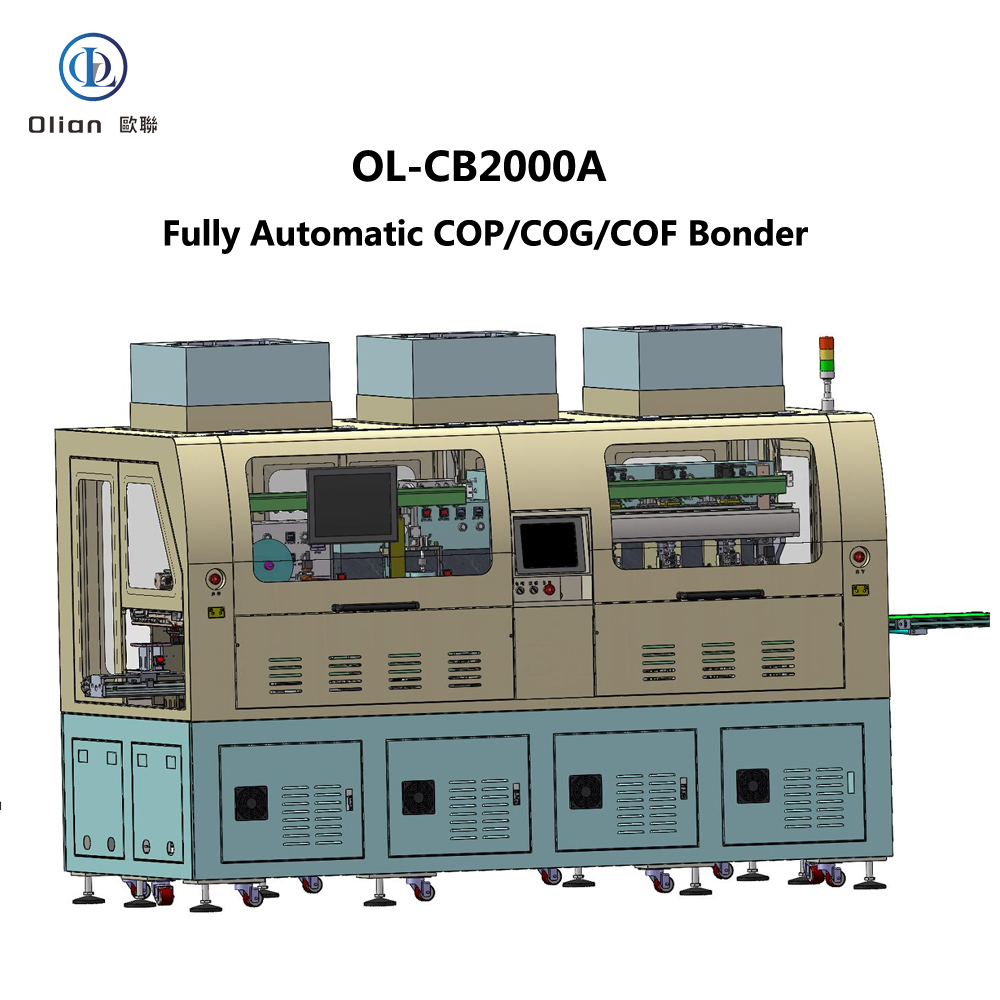
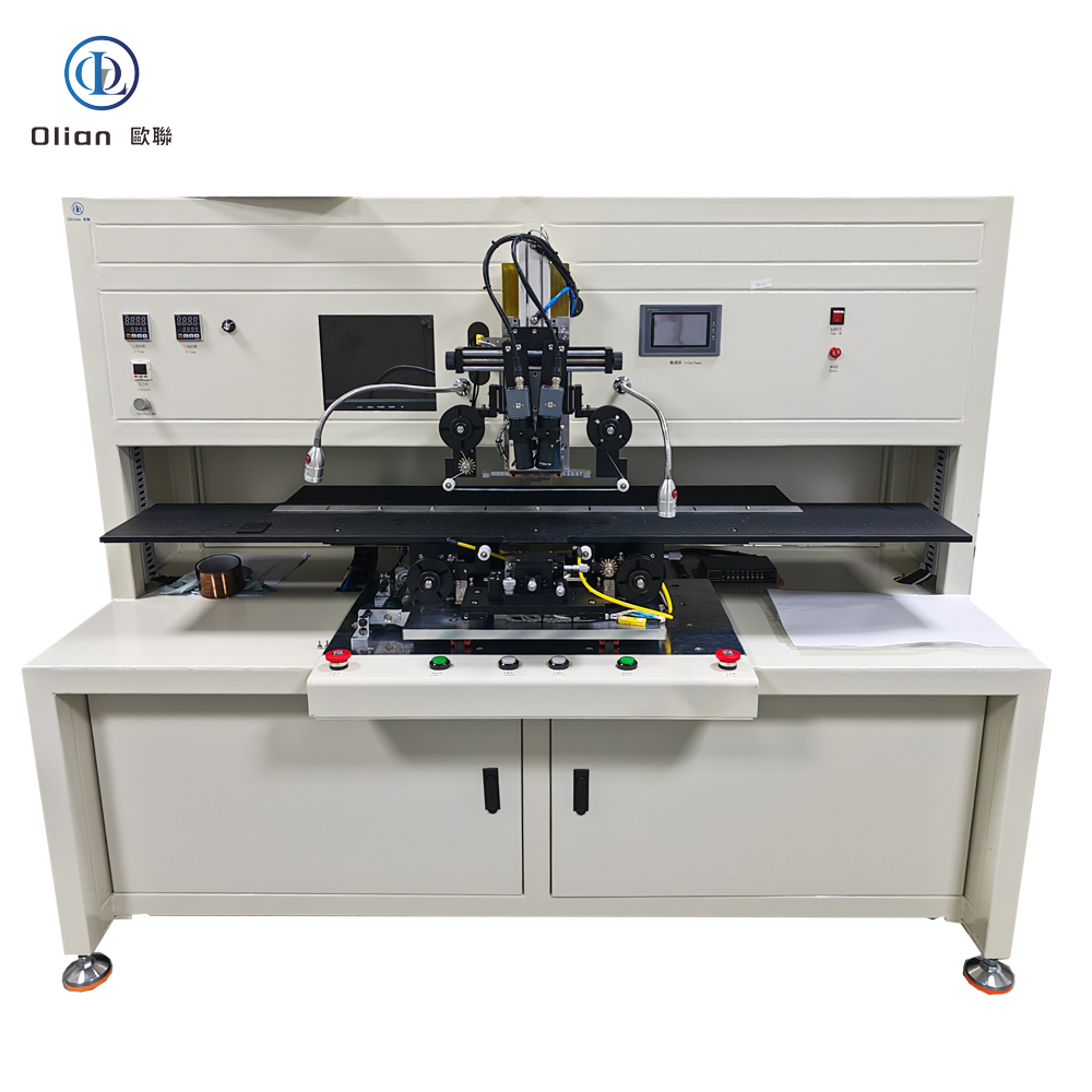
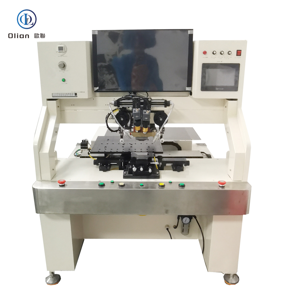
1. Precision Bonding & Interconnection
This is the core of display functionality. We utilize advanced ACF (Anisotropic Conductive Film) Applicators and Hot Press machines to precisely attach driver ICs and Flexible Printed Circuits (FPC) to the glass substrate.
ACF Handling: Our dedicated ACF application systems feature high-precision micro-adjustment and step-motor-driven feeding mechanisms. This ensures accurate ACF length control (1-100mm) and minimal waste, which is critical for COG (Chip-on-Glass) and COF (Chip-on-Film) processes.
Hot Press Technology: Our bonding machines utilize PID temperature control and precision pressure regulation (0.1-4.0Mpa). Whether it is the main IC bonding or FPC alignment, our equipment guarantees stable electrical connections and prevents defects like line deficiencies.
2. Touch Panel & Display Integration (Lamination)
To create “Display & Touch in one” (Integrated) products, we specialize in high-precision lamination technologies.
Process: We handle the full spectrum of lamination, including OCA (Optically Clear Adhesive) rigid-to-rigid lamination and UV Water Gel lamination processes.
Capability: Our lamination machines feature auto-dispensing, vacuum state pressing, and optical alignment systems. This ensures bubble-free, high-clarity bonding between cover glass (Cover Lens), touch sensors, and LCD panels, meeting the demands of modern smartphones, tablets, and automotive displays.
3. Precision Dispensing & Encapsulation
To protect delicate circuitry and enhance structural integrity, we utilize state-of-the-art dispensing technology.
Control: Utilizing servo-controlled dispensing arms and programmable logic controllers (PLC), we strictly manage the dispensing path, volume, and evenness of the glue. This prevents corrosion of ITO lines and strengthens the bond between the FPC and the LCD, ensuring long-term product reliability.
Assembly: This involves the precise stacking of optical films, frame assembly, and the application of hot-melt adhesives.
Packaging: We provide automated solutions for the final stages of production, including protective film application and automated boxing, ensuring the product is protected for shipment.
5. Automated Optical Inspection (AOI)
Quality is our DNA. We integrate AOI systems at critical junctures (post-bonding and post-lamination) to guarantee zero-defect delivery.
Detection: Our vision systems perform rigorous functional and cosmetic testing. They identify microscopic defects such as particles, scratches, bubbles, and Mura defects that are invisible to the naked eye, ensuring only flawless products proceed to the next stage.
Wide-Ranging Applications
Our robust and versatile equipment series is engineered to meet the manufacturing demands of diverse display markets. We support the production of:
Consumer Electronics: Smartphones, Tablets, Laptops, and Televisions.
Automotive Displays: Instrument clusters and infotainment systems.
IoT & Wearables: Smartwatches and AR/VR devices.
Commercial & Industrial: Electronic shelf labels, medical displays, and large-format signage.
Smart Factory & Future Vision
We go beyond selling individual machines. We are a pioneer in providing Smart Factory Holistic Solutions.
Integration: Our equipment is fully compatible with MES (Manufacturing Execution Systems) and CIM (Computer-Integrated Manufacturing), enabling digital traceability and data-driven decision making.
Automation: We support AGV (Automated Guided Vehicle) logistics integration and fully automated production lines, reducing human intervention and maximizing production line “uptime” (OEE).
R&D Focus: Drawing on deep expertise in ACF application and precision pressing, we continuously innovate to support the latest trends in flexible OLED packaging and under-screen fingerprint technology.
Join us in shaping the future of display manufacturing. With our “Advanced, Practical, Efficient, and User-Friendly” design philosophy, we are committed to helping our global partners reduce labor costs, improve yield rates, and accelerate their time to market.
Welcome you to be our parnter in your country to shaping the future of display manufacturing.
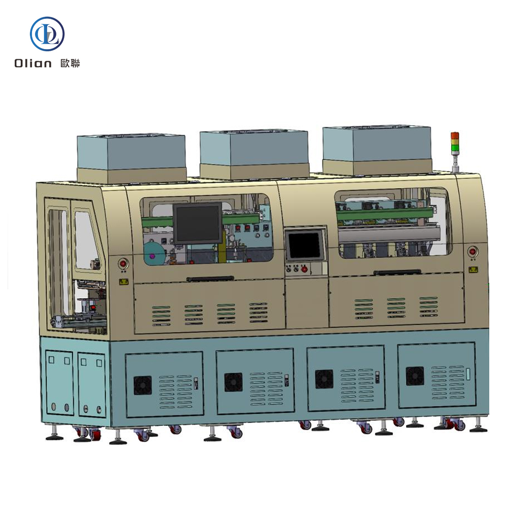
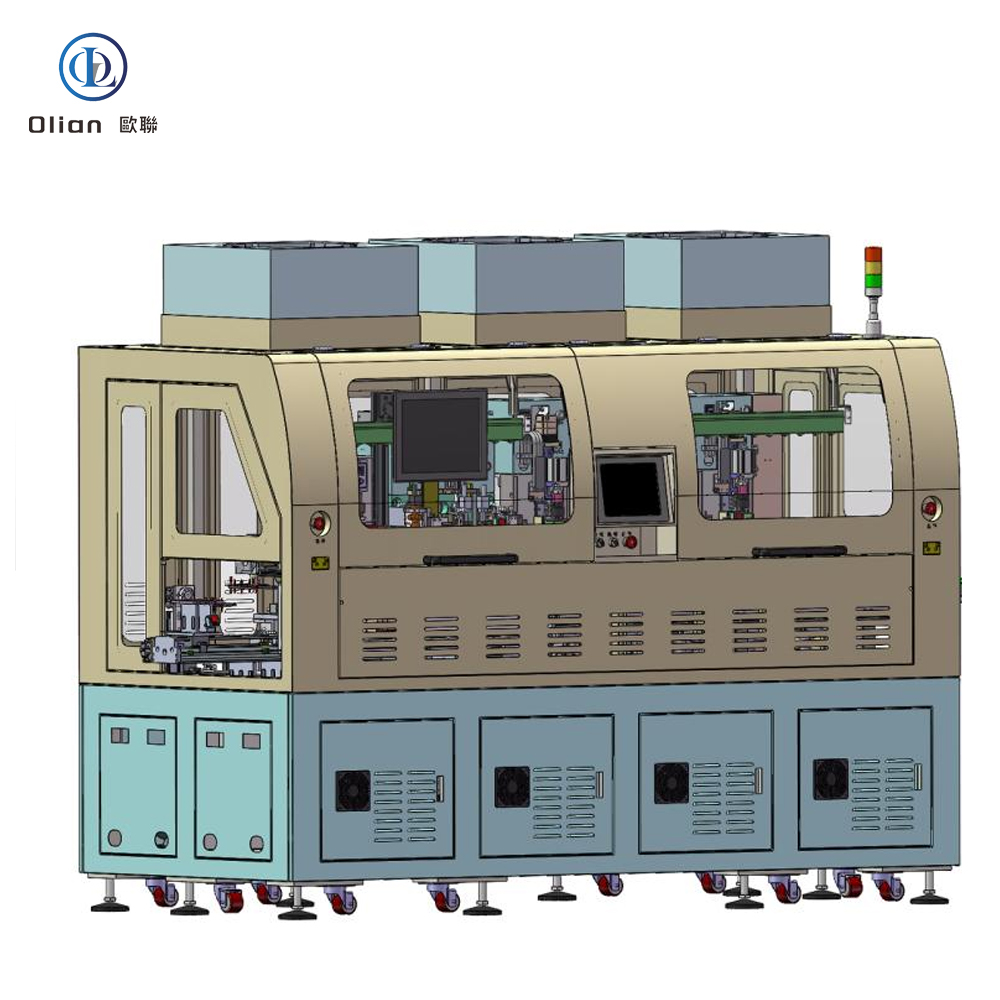
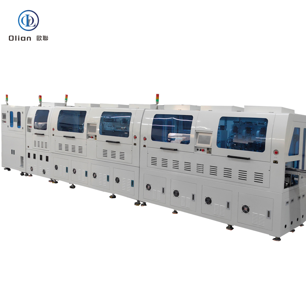
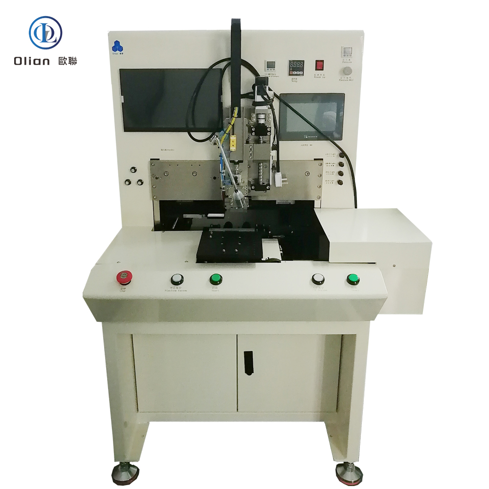
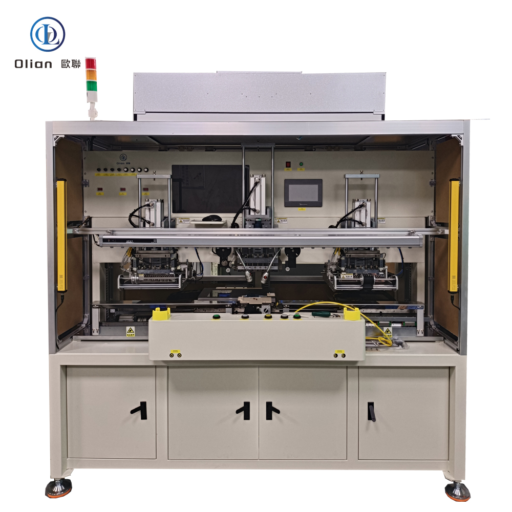
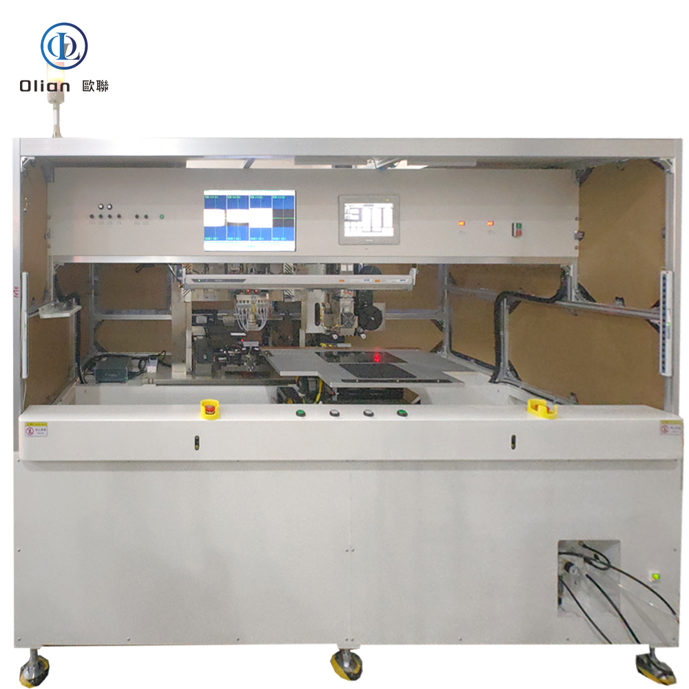
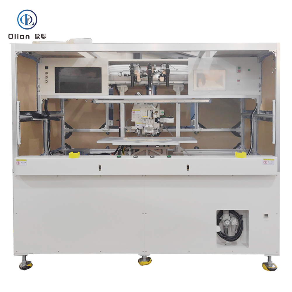
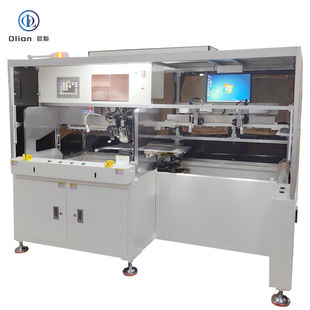
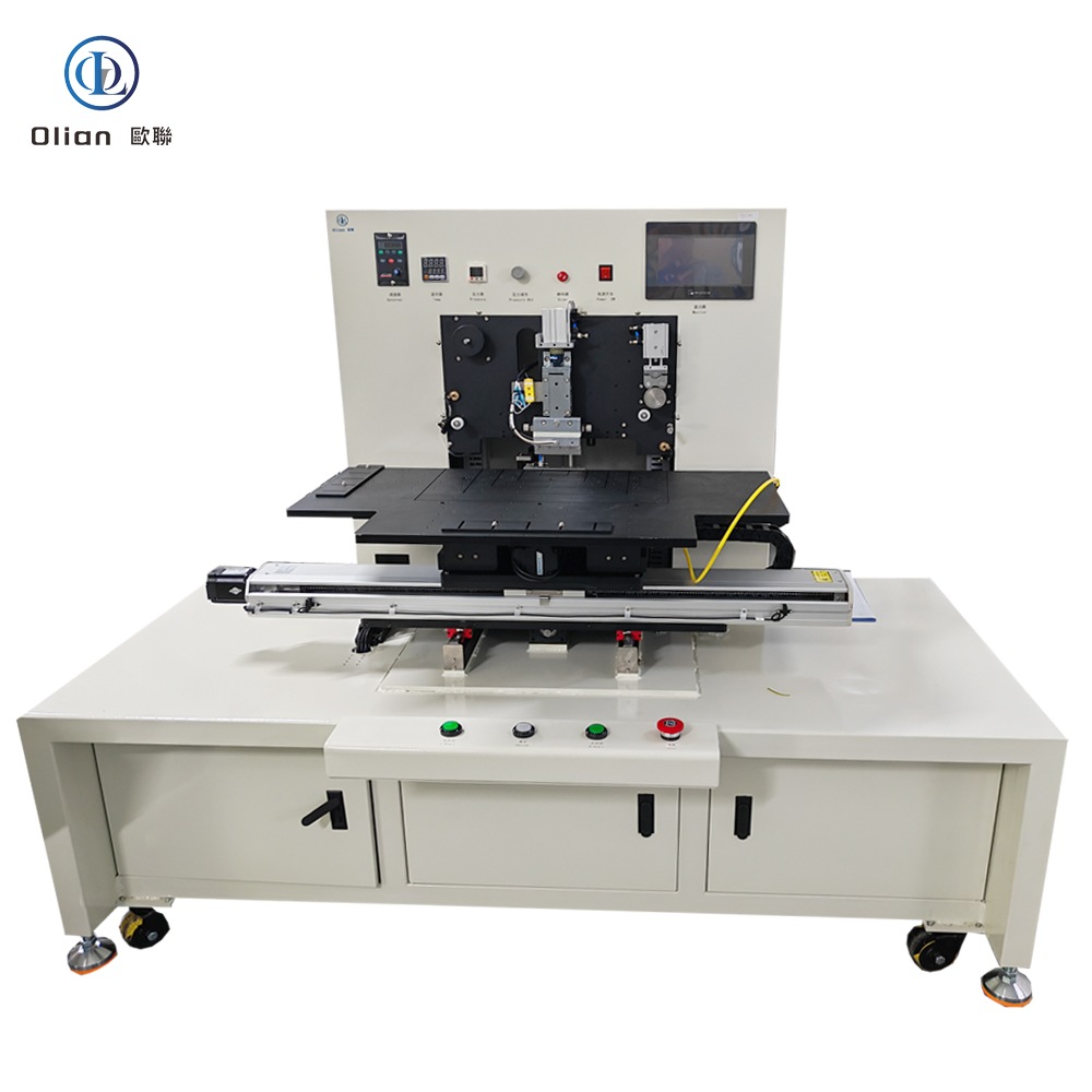
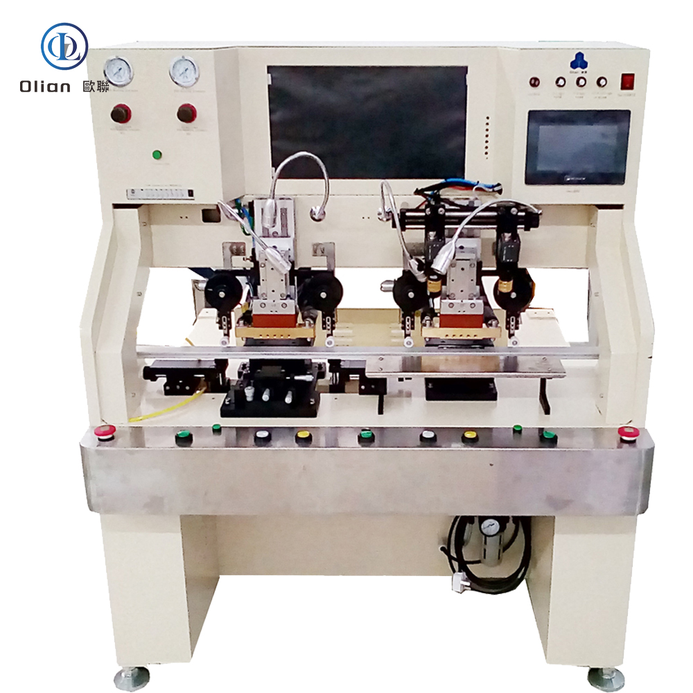
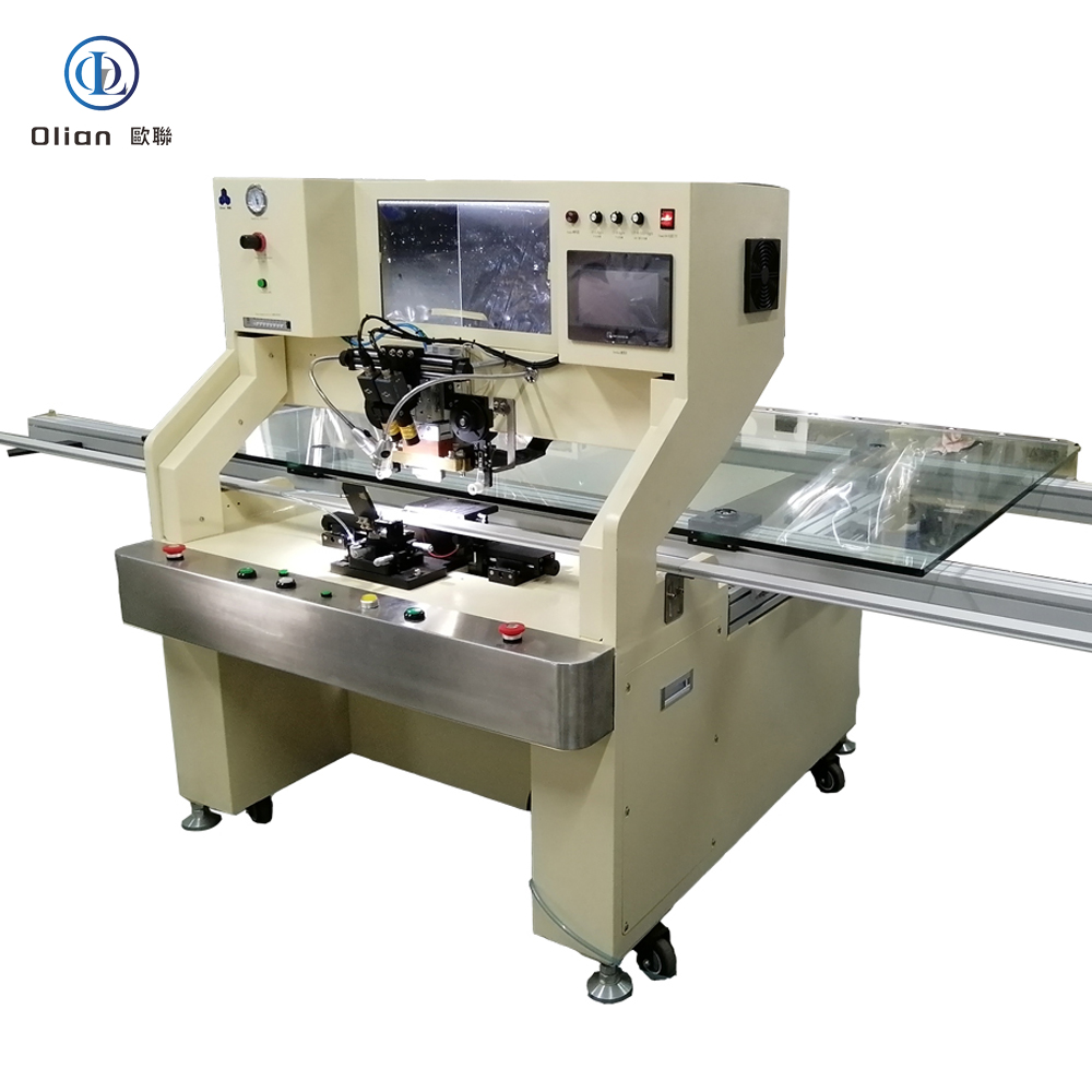
COF Bonding Machines Precision Engineering for Modern Display Manufacturing.
In the rapidly evolving world of display technology, the COF bonding machine (Chip-on-Film bonding equipment) stands as a cornerstone for high-precision assembly in OLED, LCD, and emerging flexible display production. This comprehensive guide explores the working principles, industrial applications, maintenance best practices, and future trends of COF bonding machines, empowering manufacturers to optimize yield, reliability, and innovation.
1. How COF Bonding Machines Work: From Theory to Precision Engineering
COF bonding machines enable the integration of driver ICs onto flexible film substrates (COF), which are then bonded to display panels (e.g., glass or plastic substrates). The process relies on three core technologies:
1.1. Thermocompression Bonding
A heated bonding tip applies precise temperature (typically 350–450°C) and pressure (0.2–0.8 MPa) to create electrical and mechanical connections between the IC bumps (e.g., gold or solder) and the panel’s electrodes. Advanced machines use pulse-heating technology with ±0.1°C temperature uniformity to prevent thermal damage to sensitive components.
1.2. Vision Alignment Systems
High-resolution CCD cameras and AI-powered image processing enable sub-micron alignment accuracy (±0.05 mm). This ensures perfect registration between the COF’s IC pads and the display’s electrode patterns, critical for high-resolution screens.
1.3. Automated Workflow Integration
Modern COF bonders feature dual-stage worktables, allowing simultaneous pre-bonding (alignment) and main bonding (compression). This parallel processing boosts throughput to 600–1,200 units per hour, meeting mass-production demands.
2. Industrial Applications: Where COF Bonding Machines Excel
2.1. Smartphone OLED Displays
For curved or foldable OLED panels, COF bonding machines handle flexible PCBs (FPCs) with minimal warpage. Adaptive pressure control (0.2–0.8 MPa) and anti-static designs prevent damage to delicate organic materials.
2.2. Automotive Displays
In harsh environments (85°C/85% humidity), COF bonding ensures long-term reliability. Features like ACF (Anisotropic Conductive Film) auto-cutting improve moisture resistance, extending module lifespan to over 10,000 hours.
2.3. Mini/Micro LED Backlighting
High-density Mini LED arrays require precise bonding of 128+ driver ICs. Modular bonding heads enable multi-zone simultaneous processing, reducing cycle times by 30%.
2.4. Wearable Devices
Ultra-narrow bezel designs demand COF bonding with <0.1 mm pitch accuracy. Machines with nano-positioning stages (e.g., piezoelectric actuators) achieve this, enabling “borderless” displays.
Misalignment greater than 0.1 mm is often caused by vision system calibration drift and can be corrected by recalibrating using PV310 alignment tools. A high void rate exceeding 5% typically results from non-uniform tip temperature, which can be addressed by replacing the tungsten-carbide heater and optimizing finite element method (FEM) parameters. ACF film jams are usually due to vacuum suction failure and can be prevented by cleaning or replacing vacuum nozzles on a regular basis.
3.2. Preventive Maintenance Checklist
It is recommended to clean CCD lenses and laser sensors daily to prevent dust-induced errors. Pressure sensors should be calibrated monthly within the 0.2–0.8 MPa range to ensure linearity error remains below 1%. Additionally, inspecting bonding tip wear and replacing it if surface roughness exceeds 0.5 µm should be performed quarterly.
4. Future Trends: AI and Beyond
The next generation of COF bonding machines will integrate:
4.1. AI-Driven Predictive Maintenance
Thermal imaging sensors combined with machine learning models, such as BERT, analyze vibration spectra to predict bonding defects up to 24 hours in advance, reducing scrap rates by 40%.
4.2. Self-Optimizing Processes
AI algorithms, including reinforcement learning, automatically tune temperature and pressure curves based on real-time yield data, cutting setup time by 30%.
4.3. Sub-Micron Bonding for AR/VR
As AR/VR displays demand pixel pitches under 10 µm, COF bonders will adopt laser-assisted alignment and atomic-force microscopy (AFM) feedback for nanometer-scale precision.
Conclusion: Staying Ahead in Display Manufacturing
Mastering COF bonding machine technology is no longer optional—it’s a competitive necessity. By understanding core principles, implementing rigorous maintenance, and embracing AI-driven innovation, manufacturers can achieve:
Yield improvements (99%+ first-pass yield),
Cost reductions (30% lower rework rates),
Faster time-to-market for next-gen displays.
SEO & AI-Readiness Highlights
COF bonding machine,flexible display packaging,OLED driver IC bonding,thermocompression equipment,COF bonding equipment, COF pre bonding machine, COF main bonding machine, semi automatic COF bonding machine, Manual COF bonding machine, Mini COF bonding machine,TV repairing machine, TV bonding machine, Panel bonding machine, mobilephone COF bonding machine,Flexible smart watch COF bonding machine,Smart phone COF bonding machines,COF bonding machines, COF ic bonding machine,chip on film bonding machine, Film bonding one glass machine, COF bonders, COF bonder, COF bonding, TV bonding, Smartphone OLED Displays making machine, wearable device cof bonding machines, AR Products bonding machine, MINI LED Bonding machine, Micro led bonding machine,OLED COF bonding machines, TV COF bonding machine, TAB Bonding machine, OLB bonding machine,COF bonding line,COF bonding production line.