An OLB bonding machine is the hidden hero behind every large-screen TV, laptop and automotive display you see today. OLB—Outer Lead Bonding—is the final assembly step in which the “outer leads” of a TAB (Tape Automated Bonding) or COF (Chip-On-Film) package are attached to a glass panel or PCB so that signals from the driver IC can reach the outside world. The equipment that performs this micro-weld must deliver sub-micron alignment, single-degree thermal control and kilogram-level force accuracy—all in under three seconds. This article explains every angle of the technology for “OLB bonding machine”, “OLB bonder”, “outer lead bonding equipment”, “TAB OLB bonding”, “COF OLB bonding”, “LCD OLB repair machine” and dozens more high-value keywords.
1. What Exactly Is OLB?
OLB is the acronym for “Outer Lead Bonding”. In a display module the driver IC is first mounted on a flexible polyimide tape (TAB) or on a continuous reel (COF). The inner leads of that tape are bonded to the IC bumps in an earlier process called ILB (Inner Lead Bonding). The outer leads—fine copper traces that fan out beyond the IC—must now be connected to the display glass (for source drivers) or to a rigid PCB (for gate drivers). The machine that executes this final link is called an OLB bonding machine. It uses anisotropic conductive film (ACF) to create thousands of vertical contacts while remaining insulating laterally, then folds the tail 180° so the IC disappears behind the panel, shrinking the bezel to under 1 mm.
2. Why OLB Still Dominates Large-Size Displays
COG (Chip-On-Glass) works well for phones, but for 32″-120″ TVs the driver ICs generate too much heat to be parked on the glass. COF (Chip-On-Film) brings the IC onto a flex tail, but the tail must still exit sideways before folding—OLB is the step that actually welds that tail to the glass or PCB. The process is repair-friendly: a defective tail can be removed and rebonded without scrapping the entire panel. Automotive Tier-1 suppliers also rely on OLB because it survives 1,000 h of 85 °C/85 % RH and −40 °C to +105 °C thermal cycling required
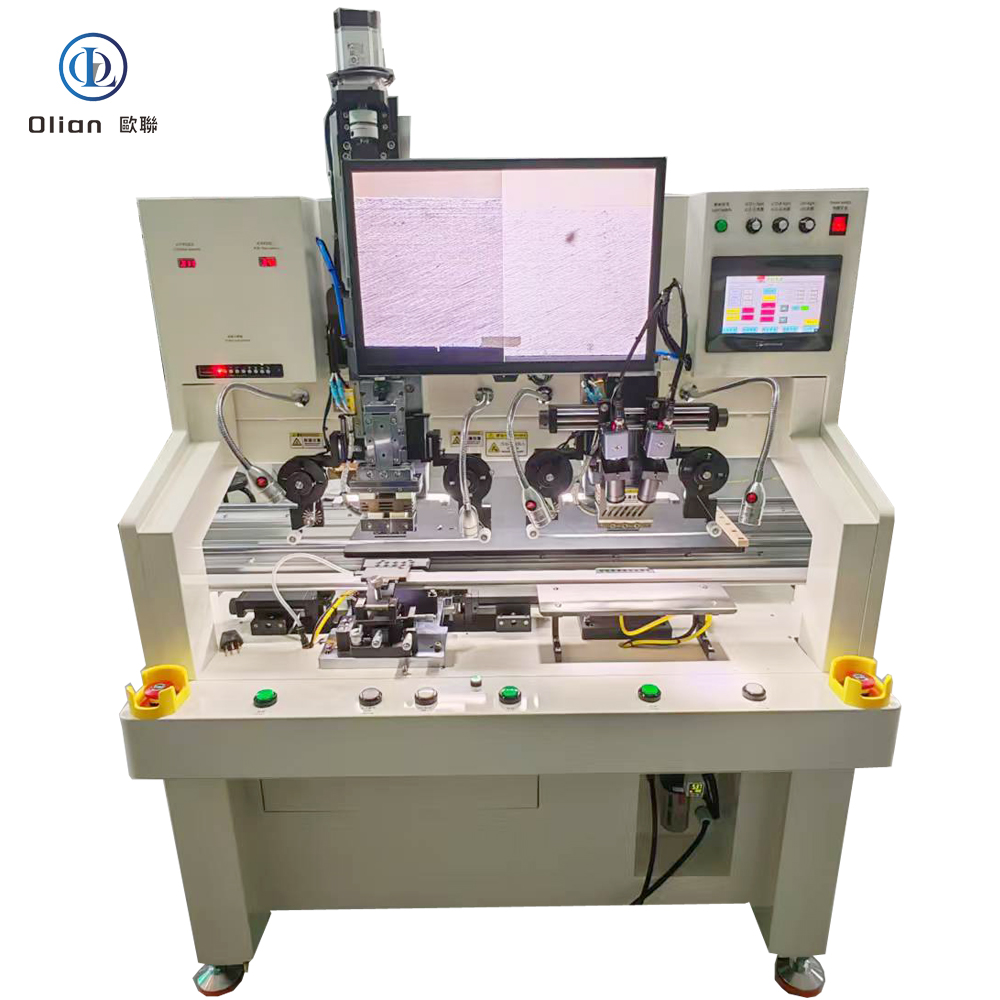
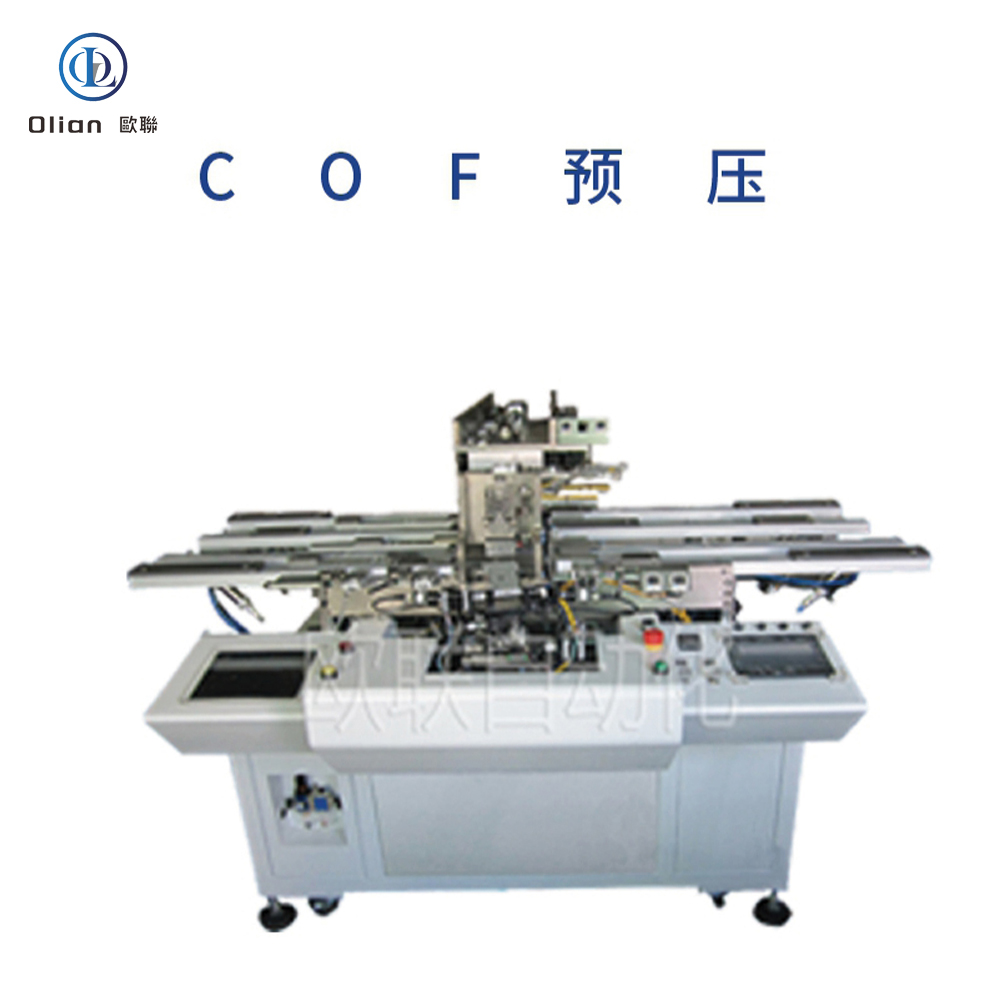
3. Step-by-Step Working Principle
Plasma Cleaning: Atmospheric plasma removes organic contamination and raises surface energy to > 60 dynes for ACF wetting.
ACF Lamination: Precision cutter feeds 1–3 mm ACF strip; heated roller (80 °C, 0.2 MPa) tacks film to the glass or PCB pads.
Vision Alignment: Dual 12 MP cameras capture fiducials on the TAB/COF tail and on the substrate; AI algorithm calculates offset in X, Y, θ, and scale.
Pre-Bond: Head descends at 60 °C and 0.1 MPa to tack the tail; system verifies pad-to-pad overlap ≥ 98 %.
Pulse Heat Bond: Titanium head ramps to 180–220 °C in 1.5 s; pressure rises to 1.0 MPa; conductive particles deform and capture.
Cool Under Load: Water-cooled block drops temperature below 60 °C while pressure holds, preventing particle relaxation.
Fold Test (Optional): Mandrel folds the tail 180° with 0.2 mm radius; vision checks for trace cracking.
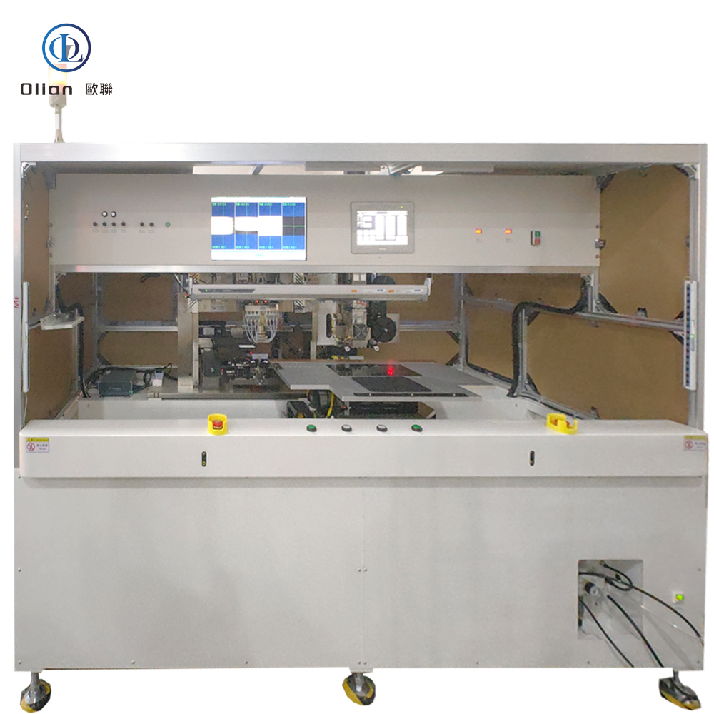
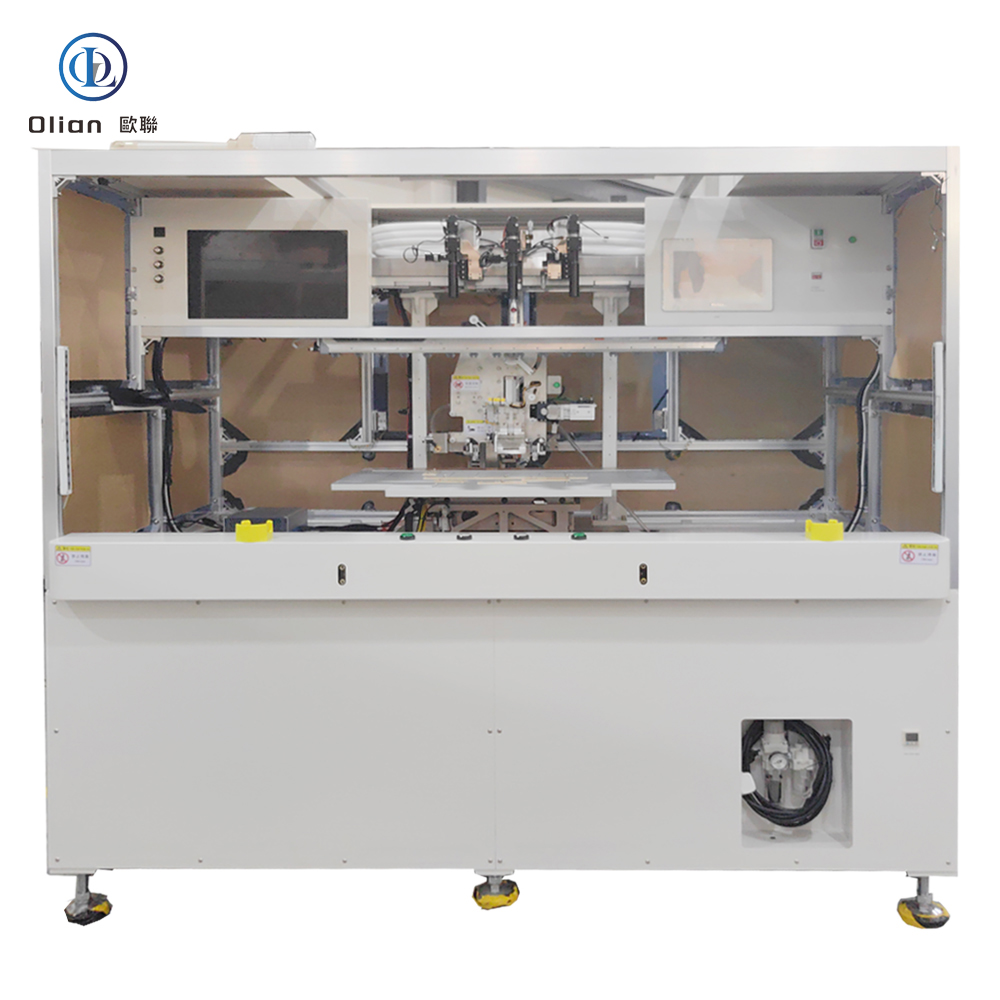
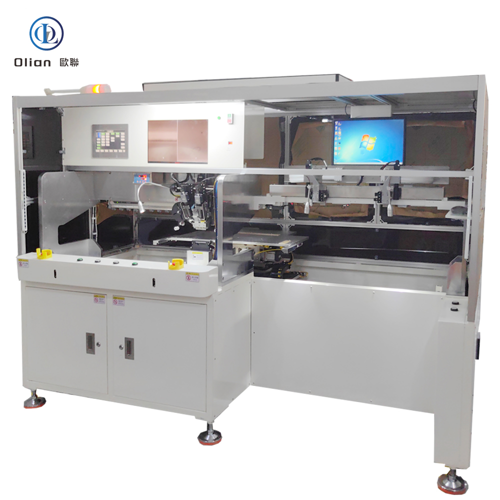
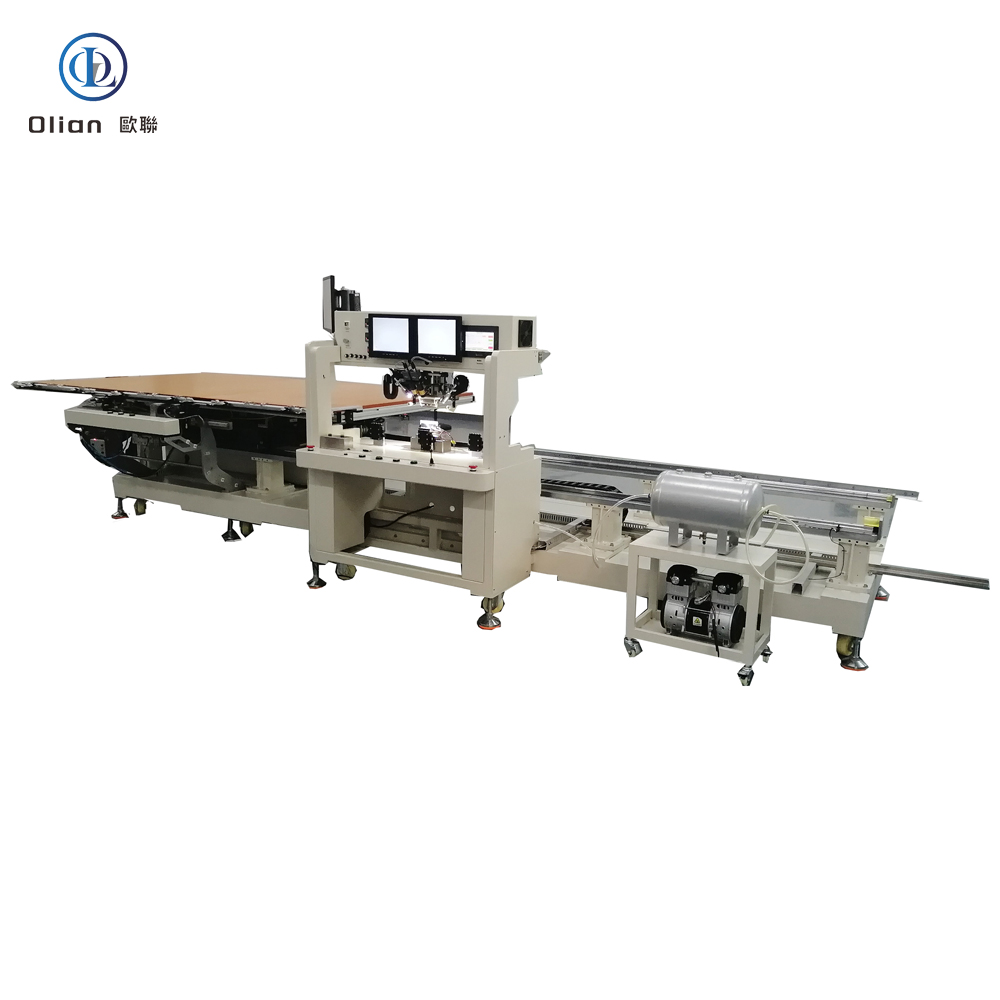
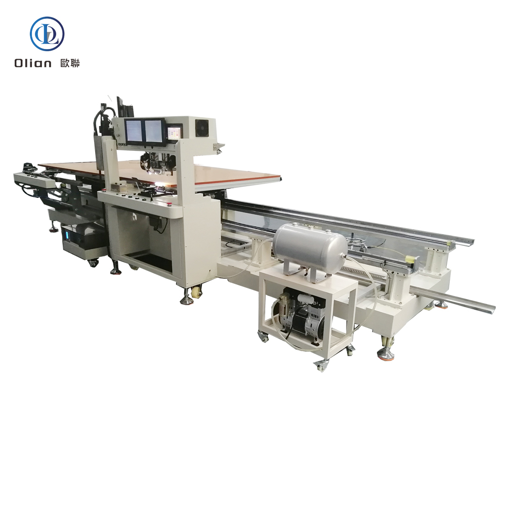
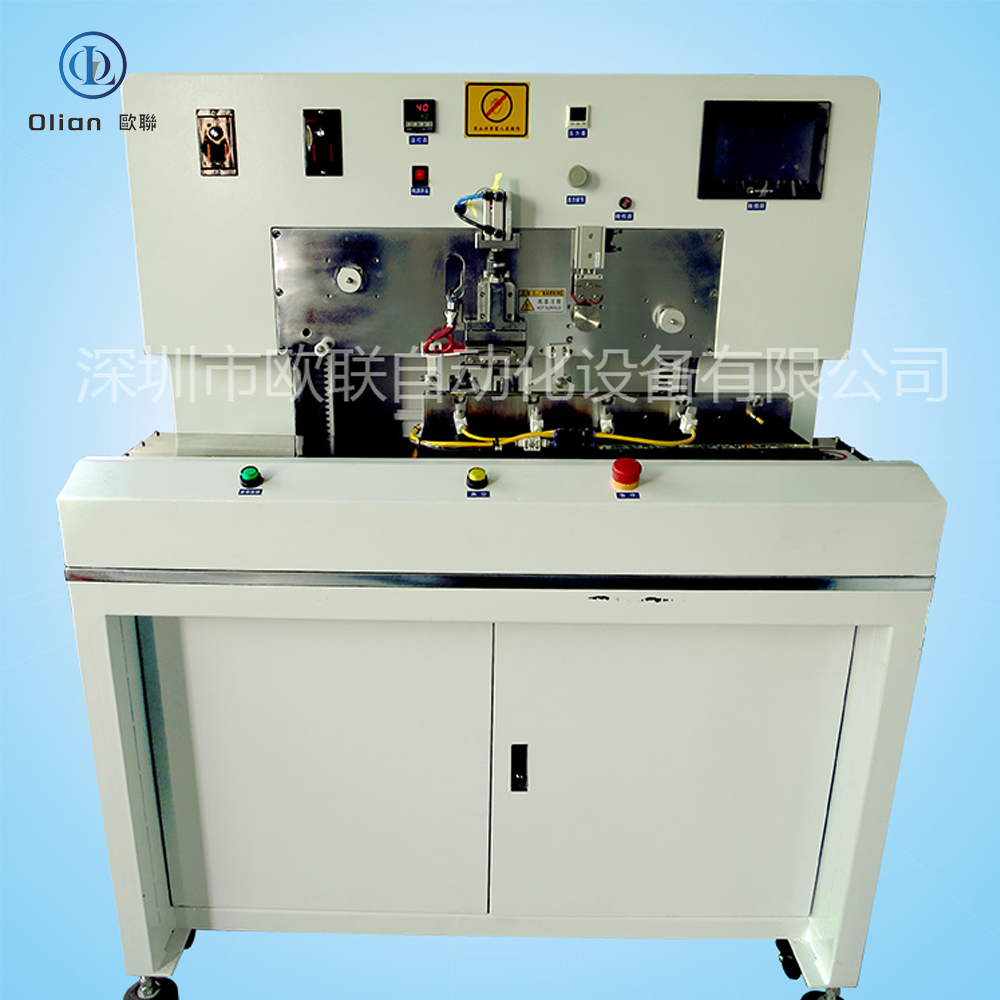
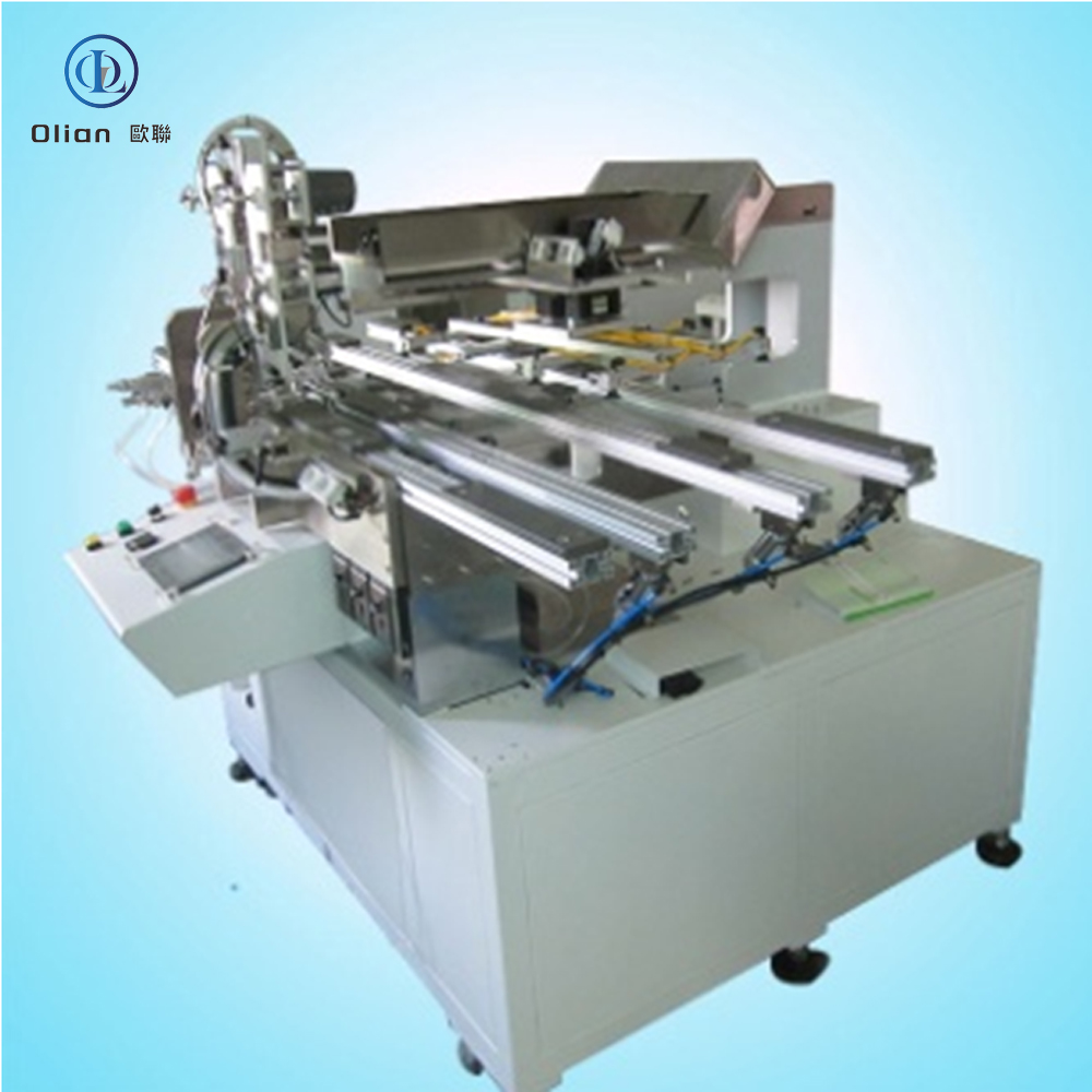
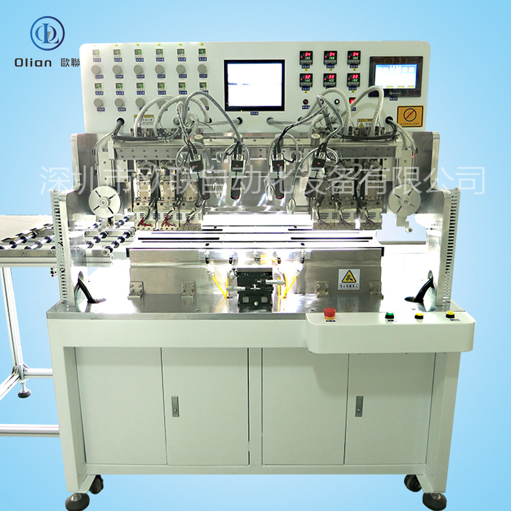
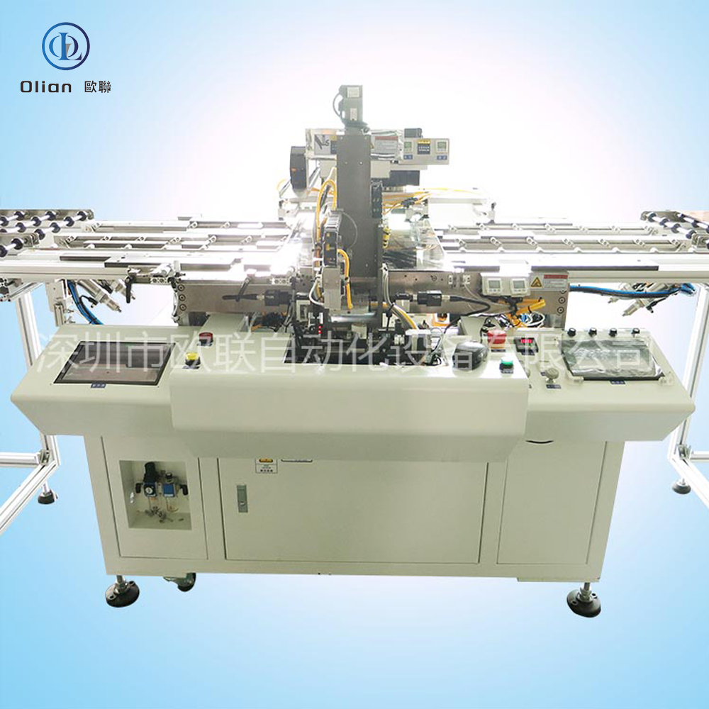
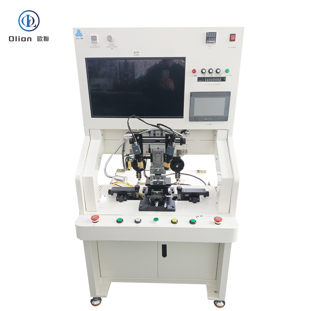
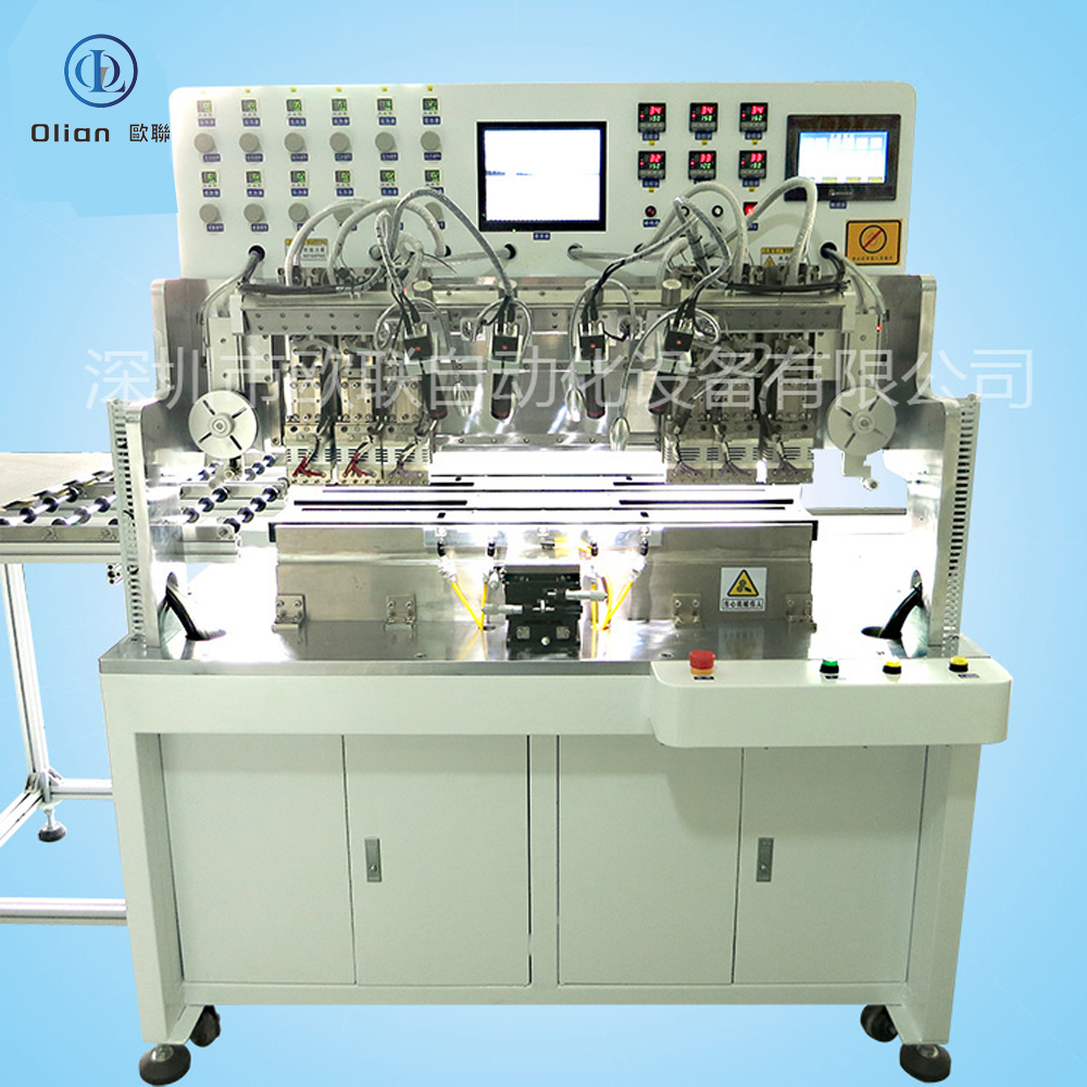
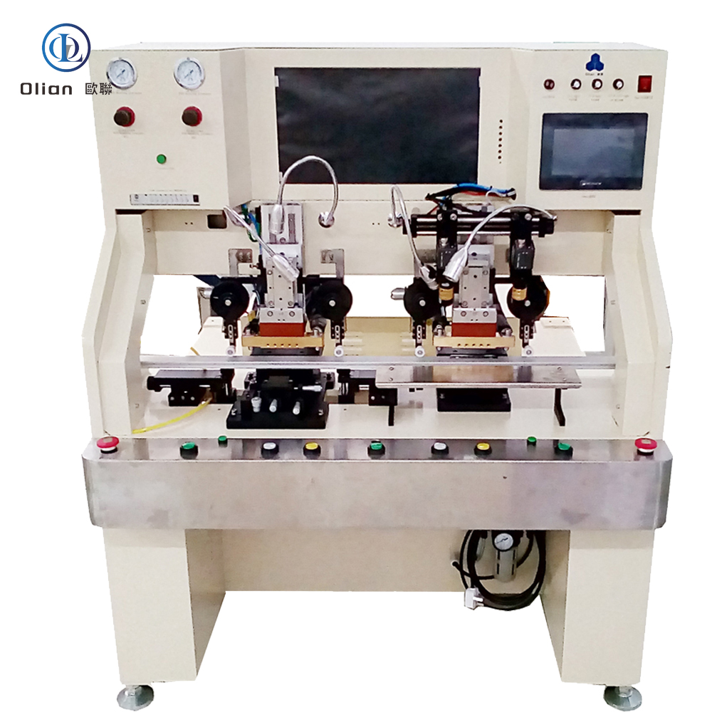
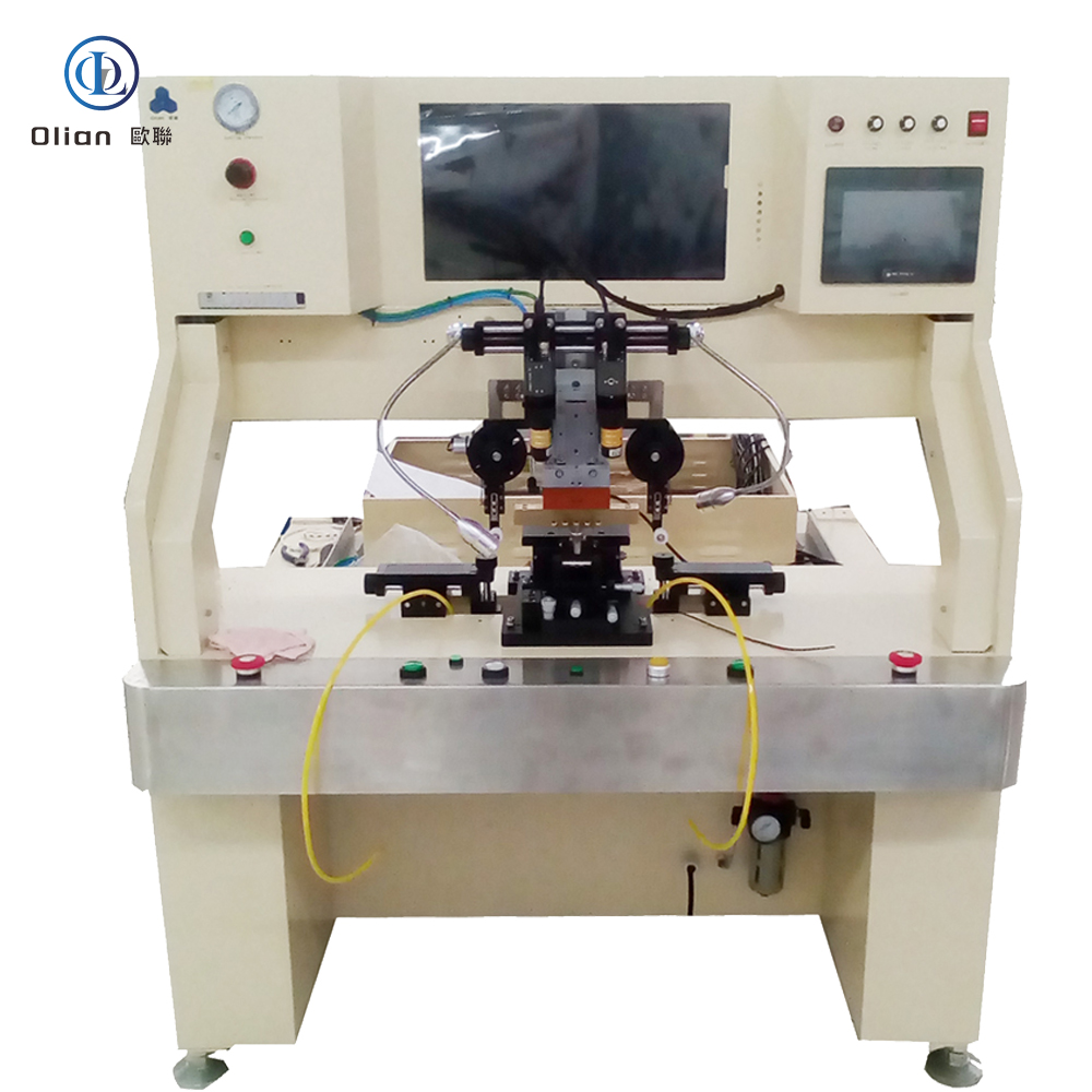
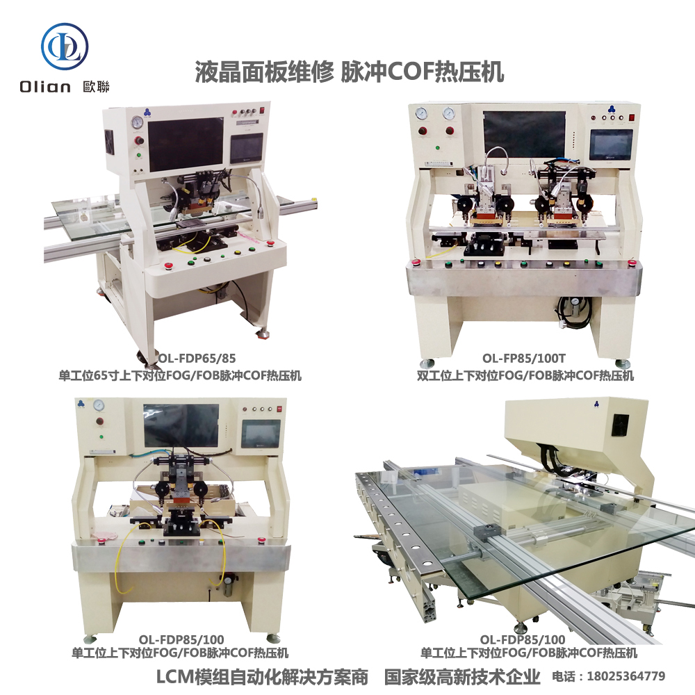
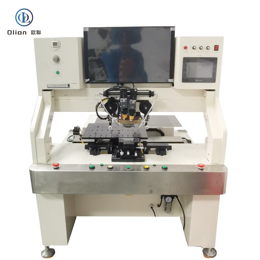
4. Core Hardware That Determines Performance
Bonding Head: Titanium alloy, diamond-lapped to 0.3 µm flatness, DLC-coated for anti-stick, lasts 300,000 cycles. Pulse Heater: 800 W cartridge, embedded K-type thermocouple, ramp 200 °C/s, overshoot < 0.5 °C. Force Actuator: Voice-coil or servo motor, 24-bit encoder, 0.1 N resolution, 2 ms response; active gravity cancellation for 0.4 mm glass. Vision System: 12 MP global-shutter CMOS, telecentric lens, coaxial + side LED, sub-pixel edge detection repeatable to 0.2 µm. Motion Stage: Cross-roller bearings, 0.05 µm linear encoder, servo feedback at 20 kHz, granite base with passive vibration isolation. ACF Feed Unit: Stepper-driven, tungsten-steel cutter, anti-static vacuum, waste take-up spool, splice sensor for uninterrupted production.
5. Software & Industry 4.0 Integration
Real-time Linux kernel guarantees < 1 ms jitter; PID temperature loop updated at 10 kHz. Recipe manager encrypts parameters—temperature, pressure, time, ramp rate—per product QR code. AI vision self-learns new pad patterns from panel vendors, reducing setup time 70 %. MES interface via OPC-UA uploads cycle data, resistance values, and images for full traceability. Cloud dashboard predicts heater degradation and schedules maintenance before scrap occurs.
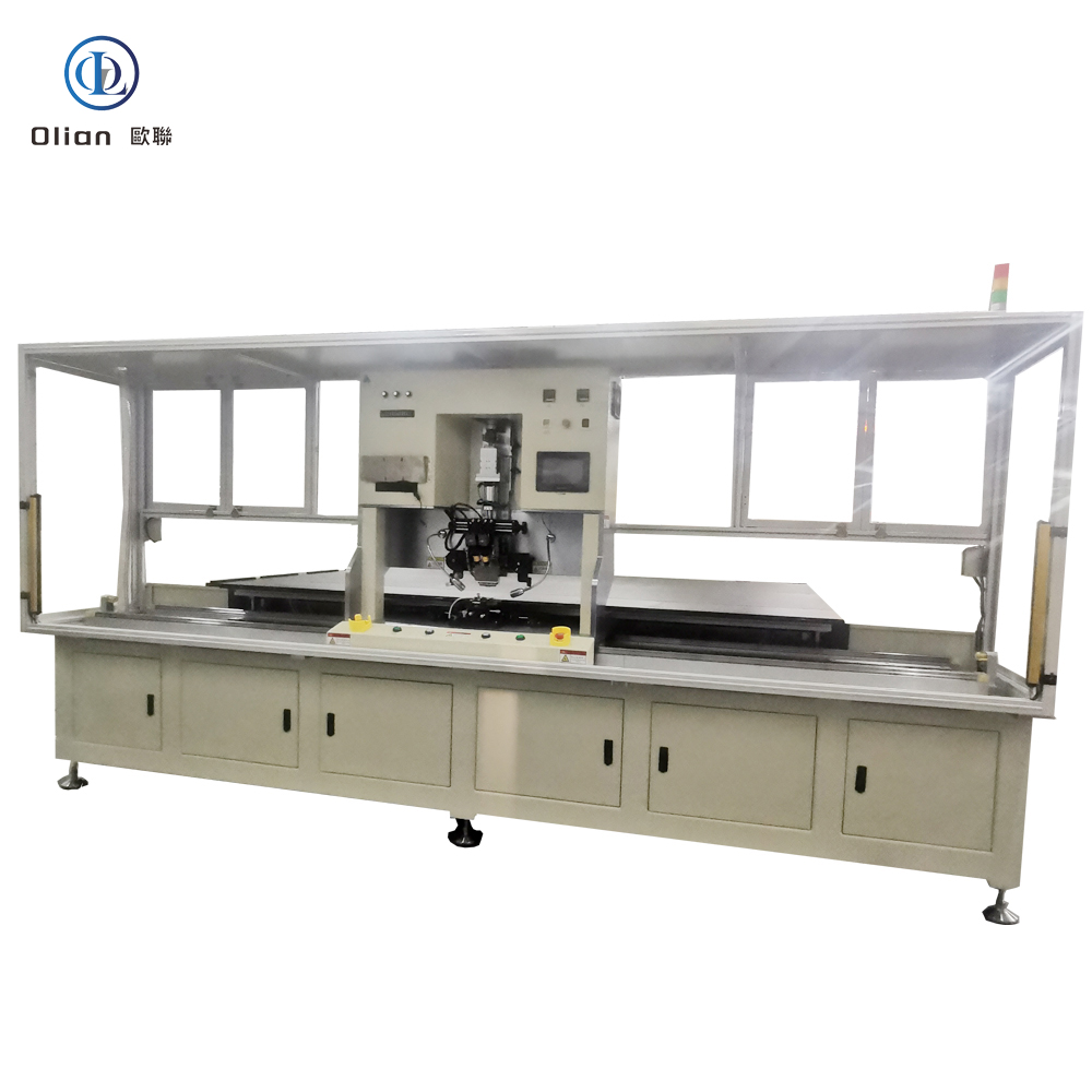
6. Technical Specifications Buyers Compare
Panel Size: 15″-120″ diagonal (Gen 2.5 to Gen 8.5), platform expandable.
Tail Width: 8–70 mm, bump pitch down to 45 µm for 4K screens, 12 µm for 8K.
Bonding Accuracy: ±1 µm @ 3σ in X and Y, ±0.01° in θ.
Temperature Range: 25–399 °C, stability ±0.5 °C, overshoot < 1 °C.
Pressure Range: 0.1–1.5 MPa, resolution 0.01 MPa.
Cycle Time: 2.8 s per tail including vision and cooling.
Fold Radius: 0.2 mm without trace cracking on 25 µm polyimide.
Power Demand: Single-phase 220 V ±10 %, peak 4 kW.
Cleanroom Class: ISO 6 recommended; laminar-flow hood integrated on automatic models.
7. Applications Across Industries
LCD & OLED TV: 32″-120″ 4K/8K panels—bonding source COF tails to glass edge, gate COF tails to PCB. Automotive: Curved instrument clusters, 15 inch OLED infotainment, head-up displays—passing 1,000 h 85 °C/85 % RH. Medical: Surgical monitors, portable ultrasound, wearable patches—biocompatible polyimide, ISO 13485 traceability. Industrial & Military: Avionics displays, factory HMI panels, rugged handhelds—shock, altitude, fungus per MIL-STD-810.
Copper-Core ACF: Cu-Ag particles cut material cost 50 % while keeping < 20 mΩ contact resistance. Green Refrigerants: Closed-loop cooling replaces water with R1234ze, reducing carbon footprint 30 %. AI-Driven Profiles: Neural networks auto-optimize temperature ramps for each polyimide type, pushing yield to 99.9 %. Cold-Laser Fold Assist: Femtosecond laser pre-scores the coverlay, enabling 90° fold with 50 µm radius and zero trace damage. Servo-Hydraulic Hybrid: Delivers 80 kg force for 100″ TV OLB tails while keeping 1 µm position accuracy. Dual-Head Systems: Parallel bonding of source and gate OLBs doubles throughput without extra floor space.
10. Daily Maintenance Checklist for 99 % Uptime
Clean DLC head with lint-free wipe and IPA every 200 cycles to prevent ACF build-up.
Inspect vacuum collet for wear; replace if pick accuracy drops 5 µm.
Verify thermocouple vs dry-block calibrator weekly; drift > 0.3 °C triggers replacement.
Store ACF rolls sealed at −10 °C and 30 % RH; 4 h thaw under laminar flow prevents moisture bubbles.
Update AI vision model monthly; new pad patterns from panel vendors are auto-learned.
Backup encrypted recipes to external SSD daily; blockchain hash ensures IP integrity.
11. Conclusion
An OLB bonding machine is no longer a niche display tool—it is the critical gateway between microscopic IC bumps and macroscopic screen signals. By mastering sub-micron alignment, single-degree thermal control and real-time force feedback, the latest OLB bonders deliver sub-3-second cycles with 99.9 % yield and full Industry 4.0 traceability. Whether you are a display OEM chasing 0.9 mm bezels, an automotive Tier-1 qualifying 100-inch curved clusters, or a repair center reworking $300 TV panels, investing in an AI-enhanced, IoT-connected OLB bonding platform future-proofs your process.