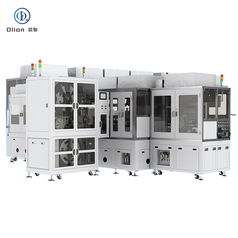
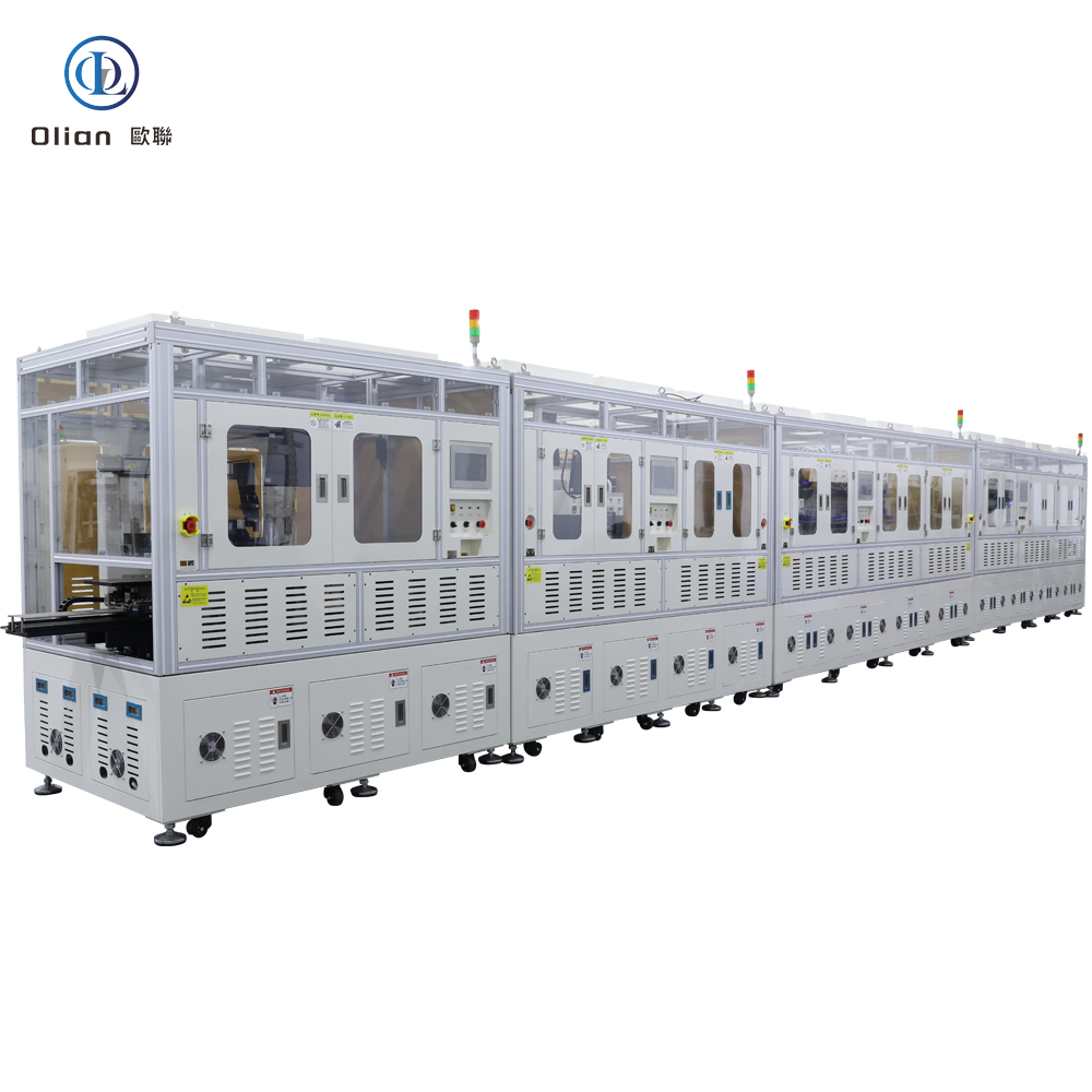
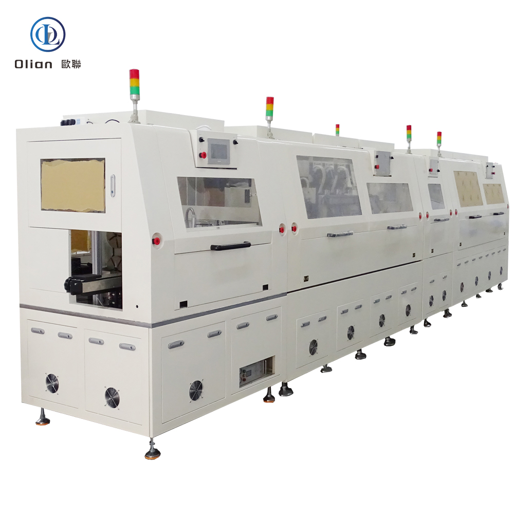
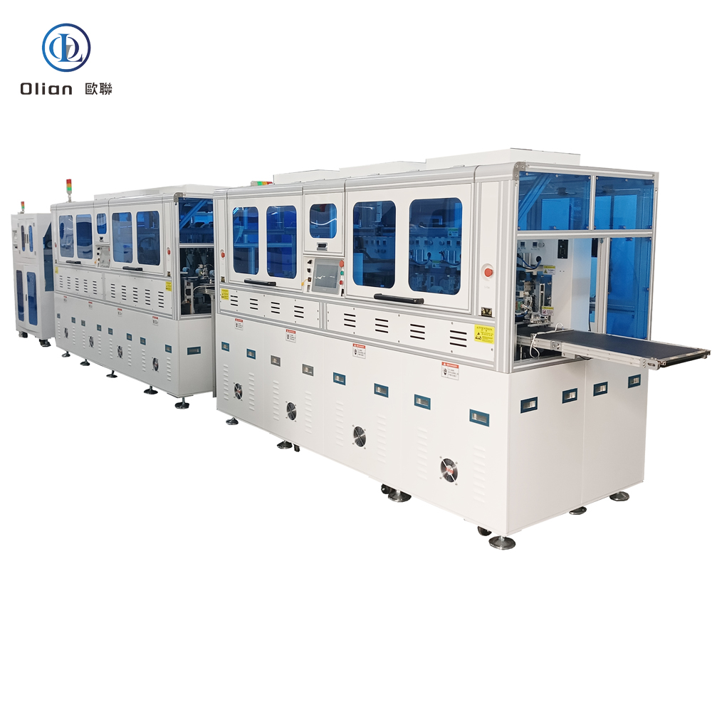
An IC bonding machine is the beating heart of every microelectronic package you touch—whether it’s the OLED display in your foldable phone, the radar sensor in your car, or the memory stack in your laptop. It is the precision system that places a bare silicon die onto a substrate—glass, flex, PCB, or lead-frame—and then creates permanent electrical joints by thermo-compression, ultrasonic, or eutectic means. Keywords”IC bonding machine”, “IC die bonder”, “wire bonding machine”, “eutectic IC bonder”, “flip-chip bonder”, “COG bonding machine”, “COB bonding machine”, “thermosonic bonding”, “ultrasonic wire bonder.
fully automatic FOG bonding machinefully automatic FOG bonding machineic bonding machinefully automatic ic bonding machineCOP BONDING MACHINECOP bonding machine
1. What Exactly Is an IC Bonding Machine?
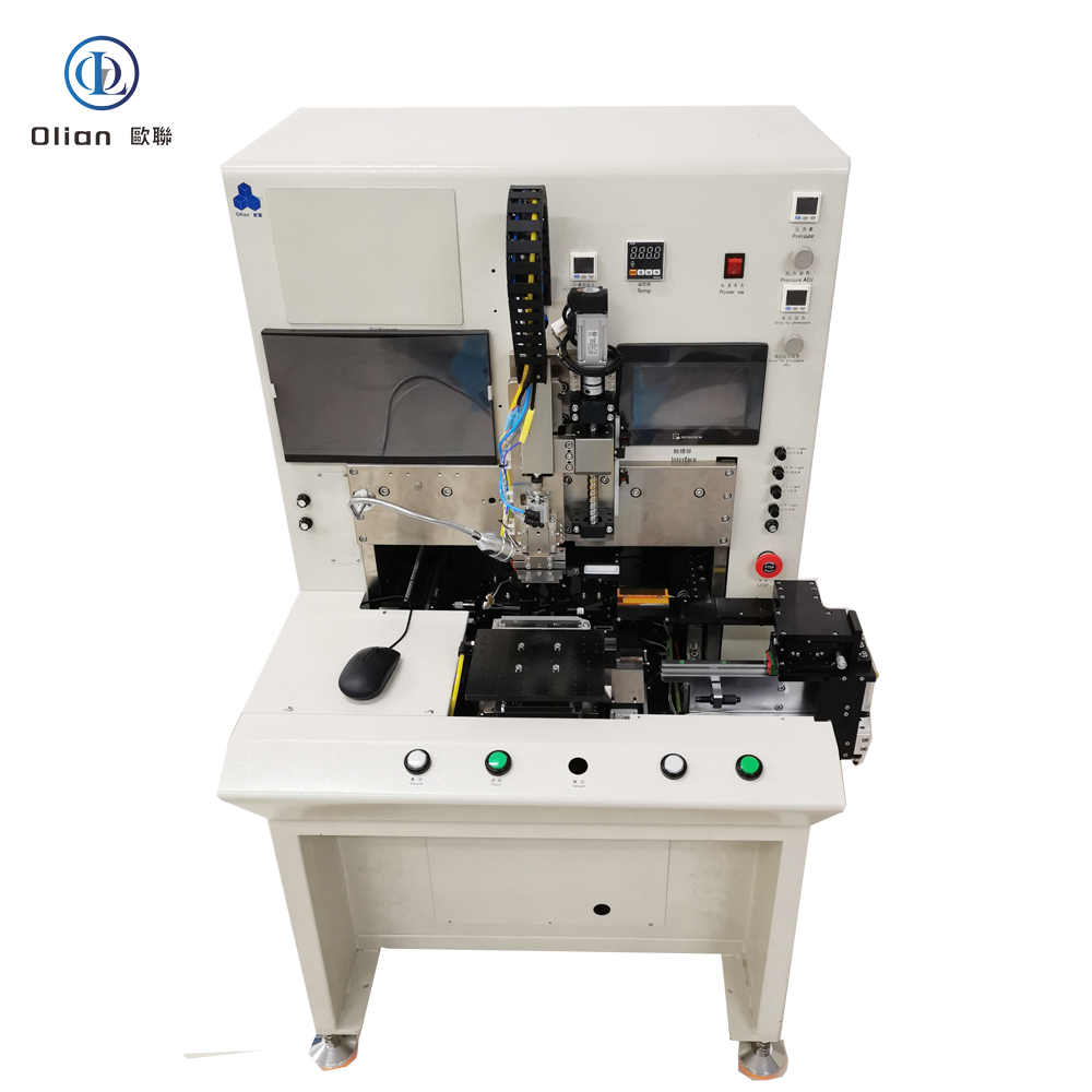
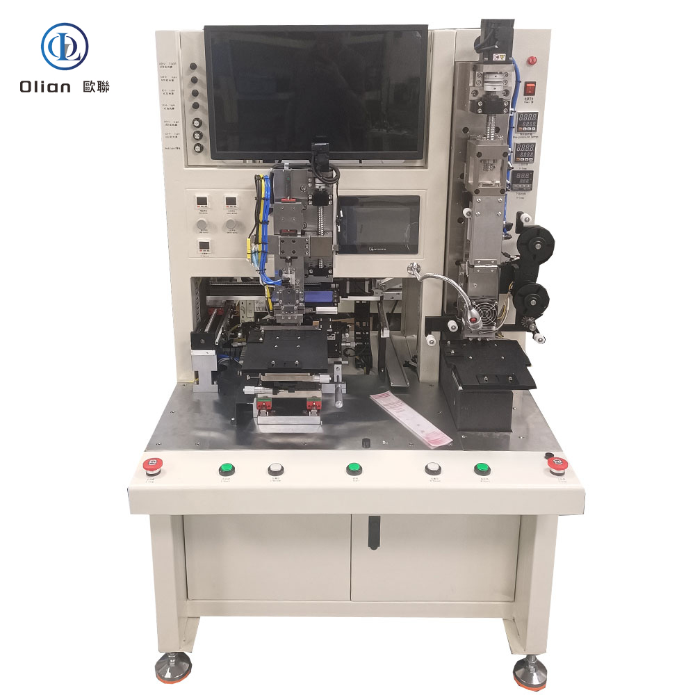
An IC bonding machine is a high-precision mechatronic platform that picks up a bare integrated-circuit die from a wafer, waffle pack, or gel-pak, places it with micron accuracy onto a target substrate, and then forms electrical and mechanical joints by one of three core methods: wire bonding (thermosonic or ultrasonic), flip-chip thermo-compression, or eutectic/solder reflow. Modern platforms achieve ±1 µm placement accuracy, ±0.3 ° angular repeatability, and 0.1 g force resolution on die sizes from 0.25 mm × 0.25 mm to 25 mm × 25 mm. The same machine also reworks defective packages by removing the old die and rebonding a new one.
2. Physics Behind the Bond: Why Heat, Force, and Ultrasound Matter
Gold or copper bumps on the die must touch copper pads on the substrate. At room temperature the native oxide layer prevents reliable contact. Thermosonic wire bonding uses 150 °C stage heat plus 60 kHz ultrasonic energy to break the oxide and form Au-Al intermetallics. Flip-chip thermo-compression applies 200 °C and 1 MPa to deform gold or solder bumps, creating cold-weld joints. Eutectic bonding raises temperature above 280 °C so Au-Sn or Cu-Sn forms a liquid phase that solidifies into a void-free joint. Each method demands closed-loop temperature, force, and time control to within 1 %.
3. Step-by-Step Working Principle (Wire-Bond Example)
Wafer Mapping: Machine vision scans the wafer, records good-die coordinates, and skips inked or cracked units.
Die Pick-Up: Ejector needles push the die upward while a vacuum collet grips it; force is kept below 50 g to avoid silicon cratering.
Die Placement: Linear motor moves the die over the substrate; bottom camera aligns fiducials; placement accuracy ±1 µm @ 3σ.
First Bond (Ball Bond): Capillary descends, forms a free-air ball, scrubs at 60 kHz, 40 g force, 150 °C for 15 ms.
Loop Formation: Capillary traces a controlled loop height (50–500 µm) to avoid shorting adjacent wires.
Second Bond (Wedge Bond): Capillary stitches the wire to the substrate pad, breaks the tail, and feeds fresh wire for the next cycle.
In-Situ Inspection: High-speed camera checks ball shape, loop height, and tail length; AI flags outliers for rework.
4. Core Hardware Modules That Determine Performance
Die Bond Head: Ceramic or titanium collet, 0.1 µm run-out, vacuum channel optimized for 50 µm thin die. Ejector Stage: Triple-needle system with 1 µm z-repeatability, adjustable stroke 0–3 mm, anti-crumple software. Linear Motors: Iron-less design, 5 g acceleration, 0.05 µm encoder resolution, backlash-free for < 1 ms settling. Force Sensor: Strain-gauge or optical, 0.1 g resolution, 10 kHz bandwidth, real-time overload protection. Temperature Stack: Pulse-heated stage 25–500 °C, ramp 100 °C/s, uniformity ±1 °C across 300 mm wafer. Vision Trains: Dual 12 MP cameras, telecentric lenses, coaxial + side LED, AI edge detection repeatable to 0.2 µm. Wire Feed System: Ultrasonic cleaner, flame-off electrode, vacuum tail collector, gold or copper wire 18–75 µm diameter.
5. Software & Control Ecosystem
Real-time Linux or RTX kernel guarantees < 500 µs jitter; PID loops updated at 20 kHz. Recipe manager encrypts parameters—temperature profile, force ramp, ultrasonic power—per product QR code. MES interface via OPC-UA uploads die ID, XY coordinates, bond force, and wire-pull data for full traceability. AI predictor analyses capillary wear and forecasts ball-shape drift 200 bonds ahead, cutting unplanned downtime 30 %. Remote VPN allows OEM engineers to debug without on-site visit, saving travel cost and CO₂ footprint.
Angular Accuracy: ±0.1° for wire bond, ±0.3° for flip-chip.
Force Range: 0.1–1000 g (wire), 10–7500 g (die attach), resolution 0.1 g.
Temperature Range: 25–500 °C, stability ±0.5 °C, overshoot < 1 °C.
Bond Time: 15 ms per wire, 3 s per flip-chip bump set, 5–25 s per eutectic die.
Wire Speed: 4–6 wires per second on modern machines.
Die Size: 0.25 × 0.25 mm to 25 × 25 mm, thickness 50–775 µm.
Wafer Size: 6″, 8″, 12″ compatible; automatic wafer change in < 60 s.
Footprint: 1900 × 1100 × 1800 mm typical, weight 1.2–2.2 t.
Power: 220 V ±10 %, 50/60 Hz, peak 4 kW.
7. Applications Across Industries
Consumer Electronics: Smartphone OLED driver, tablet touch MCU, laptop power management IC, memory stack in SSD. TV & Display: COG bonding of source drivers on 8K LCD/mini-LED panels; COF bonding on curved OLED TVs. Automotive: Radar MMIC, camera ISP, LED headlamp driver, infotainment processor—qualified to AEC-Q100 Grade 0 (−40 °C to +150 °C). Medical: MEMS pressure sensors, hearing-aid DSP, catheter imaging chip—biocompatible epoxy, ISO 13485 traceability. Industrial & Aerospace: FPGA on ceramic substrate, power GaN dies, RF amplifiers in 5G base stations, satellites, and defense systems.
8. Keyword Integration
IC bonding machine, IC die bonder, wire bonding machine, thermosonic wire bonder, ultrasonic wire bonder, eutectic IC bonding machine, flip-chip bonder, COG bonding machine, COB bonding machine, TAB bonding machine, ACF IC bonding, pulse-heat IC bonding, 1 micron placement accuracy, 12 inch wafer bonding, memory stack bonding, GaN die bonding, automotive IC bonding, medical MEMS bonding, 5G RF bonding, China IC bonding machine, automatic IC bonder, IC bonding temperature 200 C, IC bonding force 1 MPa, gold wire bonding, copper wire bonding, aluminum wire bonding.
9. Future Trends
Hybrid Bonders: Single platform switches between wire, flip-chip, and eutectic modes in < 5 min, cutting cap-ex by 40 %. AI-Driven Calibration: Neural networks auto-learn capillary wear and adjust ultrasonic power, pushing yield to 99.99 %. Copper Wire Migration: 100 % Cu wire replaces gold, cutting material cost 90 % while maintaining < 30 mΩ resistance. Cold-Laser Clean: Femtosecond laser removes organic contamination at room temperature, enabling 120 °C low-temp bonds for flexible OLED. Green Factory: Closed-loop chillers and regenerative brakes on linear motors cut energy per bond 25 %. Heterogeneous Integration: Same bonder stacks logic, memory, and RF chiplets using hybrid bonding (oxide fusion) with < 100 nm alignment.
10. Daily Maintenance for 99 % Uptime
Clean capillary with IPA every 2 h to remove aluminum smear.
Check wire-pull strength hourly; < 5 g drop triggers capillary change.
Verify thermocouple vs dry-block weekly; drift > 0.5 °C triggers replacement.
An IC bonding machine is no longer a single-purpose press—it is the atomic-level gateway between nanometer transistors and millimeter-scale packages. By mastering sub-micron placement, millisecond thermal control, and real-time force feedback, the latest IC bonders deliver 6-wire-per-second speed, 99.99 % yield, and full Industry 4.0 traceability. Whether you are a display OEM stacking 8K drivers, an automotive Tier-1 qualifying radar MMICs, or a medical start-up packaging MEMS sensors, investing in an AI-enhanced, IoT-connected IC bonding platform future-proofs your process.