Powering the Display Revolution: How Our Precision Bonding Technology Enables the Screens of Tomorrow A perspective from Shenzhen Olian Automatic Equipment Co., Ltd.
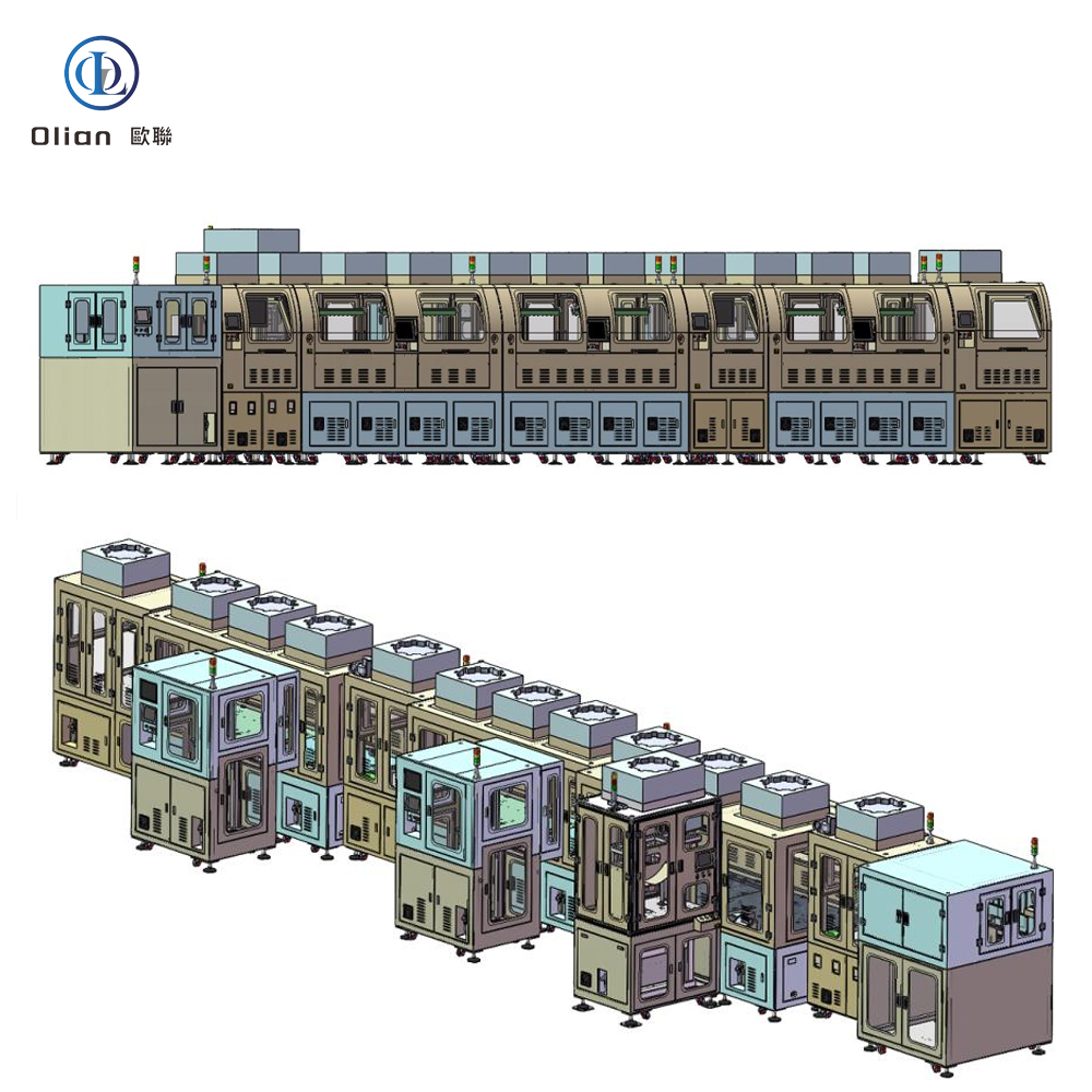
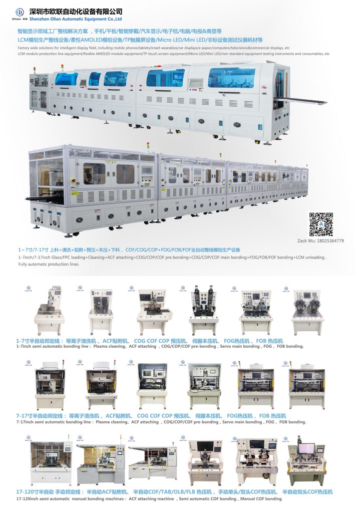
The Invisible Infrastructure of Modern Electronics Every time you unlock your smartphone, navigate your vehicle’s touchscreen dashboard, or scroll through your smartwatch, you interact with the end result of thousands of precision manufacturing processes. At Shenzhen Olian Automatic Equipment Co., Ltd., we build the machines that make those interactions possible. Since 2012, we have specialized in the critical bonding technologies that connect the microscopic components within flat panel displays. Through our platform at bonding-machine.com, we serve as the bridge between raw semiconductor components and the seamless user experiences that define modern electronics. Understanding the Technology Stack Display manufacturing requires multiple specialized bonding processes, each addressing distinct engineering challenges: ACF (Anisotropic Conductive Film) Bonding creates directional electrical pathways while maintaining insulation between adjacent circuits. This technology enables the high-density interconnects necessary for high-resolution panels without risking short circuits between closely spaced conductive traces. COF (Chip-on-Film) Bonding attaches driver integrated circuits to flexible polyimide substrates. This approach allows circuits to bend and fold—essential for curved displays and space-constrained device designs. COG (Chip-on-Glass) Bonding mounts driver ICs directly onto glass panels. This method reduces overall module thickness and improves thermal management compared to traditional PCB-based solutions. COP/FOP (Chip-on-Plastic/Film-on-Plastic) Bonding represents our contribution to the next generation of flexible and foldable displays. As consumer electronics manufacturers push beyond rigid glass substrates, our COP/FOP solutions enable entirely new form factors. Engineering for Precision and Reliability Our equipment design philosophy centers on thermal management and positional accuracy. We employ pulse heat technology rather than conventional constant heating systems. Our titanium alloy bonding heads heat instantly upon contacting the substrate, then cool while maintaining mechanical pressure. This controlled thermal profile prevents component displacement during the critical solidification phase—a common failure mode in less sophisticated systems. For alignment, we integrate dual high-resolution camera systems with adjustable LED backlighting. These vision systems achieve ±5–10 micrometer registration accuracy, ensuring perfect pad-to-pad matching even as display densities increase and pitch dimensions shrink. Our programmable logic controllers allow operators to store process recipes for different panel specifications. Whether manufacturing for Samsung, LG, BOE, or custom display architectures, our systems maintain consistent quality across product generations. Market Position and Industry Validation The global semiconductor bonding equipment market is projected to expand from $1.5 billion in 2024 to $2.8 billion by 2033, reflecting a compound annual growth rate of 7.5%. This expansion is driven by three converging trends: increasing display resolution requirements, adoption of flexible form factors, and integration of advanced displays into automotive and industrial applications. Our market position reflects sustained investment in research and development. We maintain 70+ dedicated R&D engineers and operate 4,000 square meters of precision CNC manufacturing facilities. Our intellectual property portfolio includes 10+ utility patents and proprietary software systems developed entirely in-house. Industry recognition includes designation as a National High-Tech Enterprise (2022–2025) and certification as a Specialized, Refined, Unique, Innovative enterprise (2024–2027). These credentials validate our technical capabilities and commitment to advancement. Our client relationships demonstrate real-world performance. We have delivered over 4,000 equipment units and deployed 200+ automated production lines across more than 20 regions on five continents. Our installations support manufacturing operations at BOE, CSOT, HKC, Huawei, BYD, Foxconn, and Luxshare—organizations that demand zero-defect reliability at production scale. Service as a Competitive Advantage In capital equipment industries, post-sale support often determines long-term success. We have structured our service organization to minimize customer downtime and maximize production continuity. Our technical support team guarantees 30-minute response times with true 24/7 availability. Every system ships with comprehensive installation support, operator training, and documentation. We provide a one-year warranty covering all components and labor, with lifetime service support extending well beyond the initial coverage period. Most critically, we commit to defect resolution within 30 days. If we cannot restore full functionality in that timeframe, we provide free equipment replacement or complete refund. This policy reflects our confidence in manufacturing quality and our respect for our customers’ production schedules. Future Developments and Industry Outlook Looking ahead, we see three technology trends shaping our product roadmap: MicroLED Integration requires bonding equipment capable of handling increasingly small die sizes with extraordinary placement accuracy. We are developing next-generation vision and motion control systems to address sub-10 micrometer placement requirements. Automotive-Grade Reliability demands equipment that can process larger substrates (up to 85-inch diagonal) while maintaining the same precision standards established for smartphone displays. Thermal uniformity across these expanded work areas presents significant engineering challenges we are actively solving. Laser-Assisted Bonding offers millisecond-level thermal control with localized heating that minimizes stress on adjacent components. We are integrating laser systems into our bonding platforms to enable processing of temperature-sensitive materials and structures. Conclusion The display industry continues to evolve at remarkable speed. Resolution increases, form factors multiply, and application spaces expand from consumer electronics into automotive, medical, and industrial domains. Throughout these transitions, the fundamental requirement remains consistent: reliable, precise, high-throughput bonding technology. At Shenzhen Olian, we have built our organization to meet this requirement consistently and continuously. We invite display manufacturers, equipment integrators, and technology strategists to explore our capabilities at bonding-machine.com. For specific project discussions, our engineering team is available directly at olian@szolian.com. The screens of tomorrow are being built today. We are proud to provide the precision automation that makes them possible. Shenzhen Olian Automatic Equipment Co., Ltd. is a specialized automation equipment manufacturer serving the global flat panel display and semiconductor packaging industries.
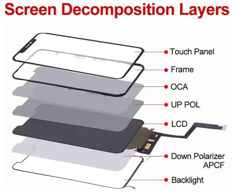
Screen Decomposition Layers: Understanding the Structure of a Modern Smartphone Display
screen decomposition layers
A smartphone screen is a sophisticated multilayered assembly that combines advanced materials and precision engineering to deliver vibrant visuals, responsive touch input, and durability. The diagram above illustrates the screen decomposition layers of a typical LCD-based smartphone display, showing how each component stacks together from top to bottom.
Touch Panel (Top Layer) The outermost layer is the Touch Panel, usually made of strengthened glass (such as Gorilla Glass). This layer detects finger touches using capacitive technology and protects the internal components from scratches, dust, and impacts. It is the surface users interact with daily.
Frame Directly beneath the touch panel is the Frame, which provides structural support and maintains the precise alignment of all layers. It helps keep the screen assembly rigid and ensures proper spacing between components.
OCA (Optically Clear Adhesive) OCA is a transparent adhesive layer that bonds the touch panel and frame to the layers below. It is optically clear to minimize light loss and prevent air gaps that could cause reflections or reduce image quality.
UP POL (Upper Polarizer) The Upper Polarizer (UP POL) is a thin optical film that controls the polarization of light passing through the LCD layer. It works together with the lower polarizer to regulate light transmission and enhance contrast and color accuracy.
LCD (Liquid Crystal Display) The LCD is the core imaging layer. It contains liquid crystals that twist or align when an electric current is applied, modulating light to create images and colors. Modern smartphone LCDs offer high resolution, excellent color reproduction, and fast refresh rates.
Down Polarizer (APCF) Below the LCD sits the Down Polarizer, also referred to as APCF (Advanced Polarizer Compensation Film). This layer further refines light polarization, improving viewing angles, reducing glare, and enhancing overall visual performance.
Backlight At the very bottom is the Backlight unit. Since LCD panels do not emit light themselves, the backlight provides the necessary illumination. It typically consists of LED lights and light-guiding plates that evenly distribute light across the entire screen, ensuring consistent brightness and clarity. Why Layered Design Matters Each layer in this decomposition serves a specific purpose: Protection and Interaction: The top layers handle user input and physical protection. Optical Performance: Polarizers and adhesives optimize light transmission and image quality. Image Formation: The LCD layer creates the actual picture. Illumination: The backlight ensures the screen is visible in all lighting conditions. Understanding these screen decomposition layers is particularly useful for technicians performing screen repairs or replacements, as damage to any single layer can affect the entire display’s performance. For example, a cracked touch panel can often be replaced separately, while damage to the LCD or backlight usually requires replacing the full assembly. This modular layered structure allows manufacturers to balance factors like thinness, durability, display quality, and production cost in modern smartphones. As display technology evolves toward OLED and foldable screens, similar layered principles continue to apply, though the specific materials and stacking order may differ.
if you also in the field of displays, you can contact us for our bonding machines for your factory. wechat/whatsapp:wa.me/8618025364779 bonding-machine.com Zack wu Shenzhen Olian